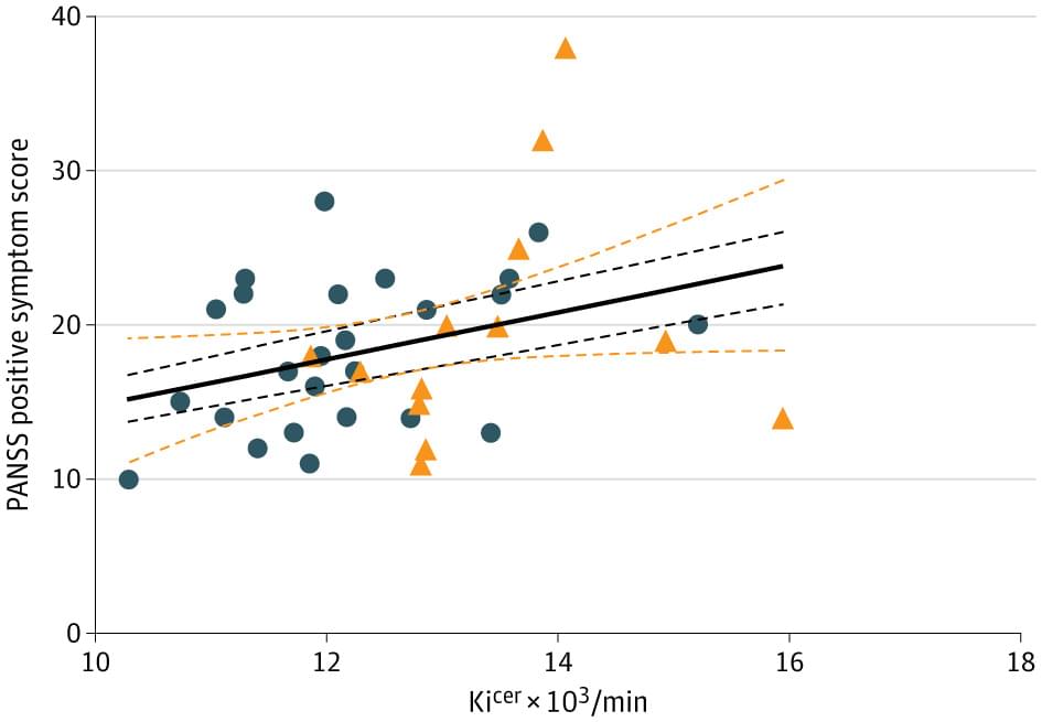
Dopamine synthesis capacity is reduced in psychosis with depression compared to mixed/mania syndromes, while positive psychotic symptoms correlate with higher dopamine synthesis in the associative striatum.
Importance There is limited neurobiological or trial evidence guiding treatment of comorbid affective syndromes in psychotic disorders. Given the use of dopamine-blocking antipsychotics, understanding dopamine function across these mood states is warranted.
Objective To test for differences in dopamine synthesis capacity (Kicer) between affective syndromes across psychotic disorders and for association with psychotic symptom severity.
Design, Setting, and Participants In this cross-sectional study using fluorine F 18–labeled fluorodopa (18 F-DOPA) positron emission tomography (PET), individuals with first-episode psychosis and comorbid affective syndromes, including a current major depressive episode (MDE) or mixed/mania syndromes, and matched controls were recruited from early intervention services in inner-city London, United Kingdom. Data were collected from March 2013 to February 2022 and analyzed from October 1, 2023, to January 1, 2025.


