Toggle light / dark theme

Checking the quality of materials just got easier with a new AI tool

Manufacturing better batteries, faster electronics, and more effective pharmaceuticals depends on the discovery of new materials and the verification of their quality. Artificial intelligence is helping with the former, with tools that comb through catalogs of materials to quickly tag promising candidates.

But once a material is made, verifying its quality still involves scanning it with specialized instruments to validate its performance — an expensive and time-consuming step that can hold up the development and distribution of new technologies.

Now, a new AI tool developed by MIT engineers could help clear the quality-control bottleneck, offering a faster and cheaper option for certain materials-driven industries.

Framework models light-matter interactions in nonlinear optical microscopy to determine atomic structure

Materials scientists can learn a lot about a sample material by shooting lasers at it. With nonlinear optical microscopy—a specialized imaging technique that looks for a change in the color of intense laser light—researchers can collect data on how the light interacts with the sample, and through time-consuming and sometimes expensive analyses, characterize the material’s structure and other properties.

Now, researchers at Pennsylvania State University have developed a that can interpret the nonlinear optical microscopy images to characterize the material in microscopic detail.

The team has published its approach in the journal Optica.

Low-power MoS₂-based microwave transmitter could advance communications

To further advance wireless communication systems, electronics engineers have been trying to develop new electronic circuits that operate in the microwave frequency range (1–300 GHz), while also losing little energy while transmitting signals. Ideally, these circuits should also be more compact than existing solutions, as this would help to reduce the overall size of communication systems.

Most of the microwaves integrated in current communication systems are made of bulk materials, such as silicon or gallium arsenide. While these circuits have achieved good results so far, both their size and have proved to be difficult to reduce further.

Two-dimensional (2D) semiconducting materials, which are made up of a single atomic layer, could overcome the limitations of bulk materials, as they are both thinner and exhibit advantageous electrical properties. Among these materials, (MoS₂), has been found to be particularly promising for the development of circuits and other components for communication systems.

Twisting sound: Scientists discover a new way to control mechanical vibrations in metamaterial

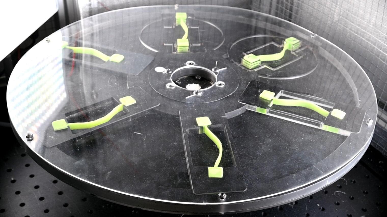
Scientists at the Advanced Science Research Center at the CUNY Graduate Center (CUNY ASRC) have discovered a way to control sound and vibrations using a concept inspired by “twistronics,” a phenomenon originally developed for electronics.

Their research, published in the journal PNAS, introduces “twistelastics”—a technique that uses tiny rotations between layers of engineered surfaces to manipulate how mechanical waves travel.

Sound and control are essential for technologies like ultrasound imaging, microelectronics, and advanced sensors. Traditionally, these systems rely on fixed designs, limiting flexibility. The new approach allows engineers to reconfigure wave behavior by twisting two layers of engineered surfaces, enabling unprecedented adaptability.

Physics-informed AI excels at large-scale discovery of new materials

One of the key steps in developing new materials is property identification, which has long relied on massive amounts of experimental data and expensive equipment, limiting research efficiency. A KAIST research team has introduced a new technique that combines physical laws, which govern deformation and interaction of materials and energy, with artificial intelligence. This approach allows for rapid exploration of new materials even under data-scarce conditions and provides a foundation for accelerating design and verification across multiple engineering fields, including materials, mechanics, energy, and electronics.

Professor Seunghwa Ryu’s research group in the Department of Mechanical Engineering, in collaboration with Professor Jae Hyuk Lim’s group at Kyung Hee University and Dr. Byungki Ryu at the Korea Electrotechnology Research Institute, proposed a new method that can accurately determine material properties with only limited data. The method uses physics-informed machine learning (PIML), which directly incorporates physical laws into the AI learning process.

In the first study, the researchers focused on hyperelastic materials, such as rubber. They presented a physics-informed neural network (PINN) method that can identify both the deformation behavior and the properties of materials using only a small amount of data obtained from a single experiment. Whereas previous approaches required large, complex datasets, this research demonstrated that material characteristics can be reliably reproduced even when data is scarce, limited, or noisy.

Stable ferroaxial states offer a new type of light-controlled non-volatile memory

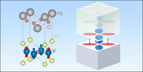
Ferroic materials such as ferromagnets and ferroelectrics underpin modern data storage, yet face limits: They switch slowly, or suffer from unstable polarization due to depolarizing fields respectively. A new class, ferroaxials, avoids these issues by hosting vortices of dipoles with clockwise or anticlockwise textures, but are hard to control.

Researchers at the Max-Planck-Institute for the Structure and Dynamics of Matter (MPSD) and the University of Oxford now show that bi-stable ferroaxial states can be switched with single flashes of polarized terahertz light. This enables ultrafast, light-controlled and stable switching, a platform for next-generation non-volatile data storage. The work is published in the journal Science.

Modern society relies on , where all information is fundamentally encoded in a of 0s and 1s. Consequently, any physical system capable of reliably switching between two stable states can, in principle, serve as a medium for digital data storage.

Bandages Made From Living Fungi Could Be The Future of Wound Healing

Fungi are best known for returning dead, organic matter to the Earth, but materials scientists are exploring whether they could someday help our bodies repair, in the form of special hydrogels.

To play a role in biomedical settings, a hydrogel needs a multilayered structure like our own skin, cartilage and muscles. While some engineers are working on synthetic versions that mimic biology, University of Utah scientists have found a hydrogel that literally has a life of its own.

Marquandomyces marquandii is a common species of soil mold, and a promising candidate for the job. This fungus has had a bit of an identity crisis, being misclassified as Paecilomyces marquandii until it was reassigned to its own genus in 2020. Soon, it may be able to add the role of ‘bio-integrated hydrogel’ to its resume.

/* */