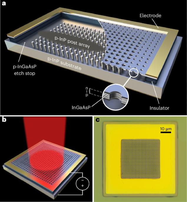
A monolithic architecture allows electrical injection of carriers into photonic structures without perturbing the optical mode.
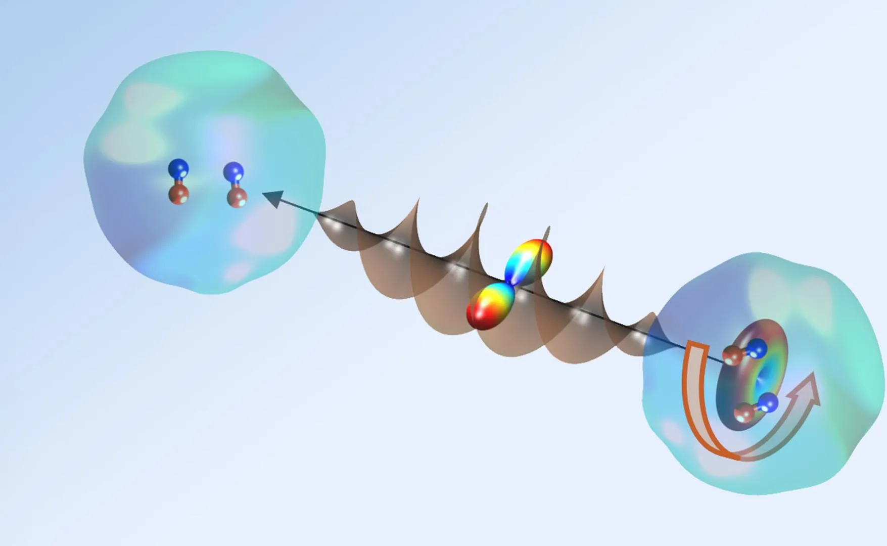
Physicists have developed a new way to control the rotation of molecules inside tiny droplets of liquid helium, marking an important advance in the study of superfluids. By using a specially designed optical centrifuge, the team was able to precisely spin molecules suspended in liquid helium nano-droplets, giving scientists a powerful new tool for exploring these unusual frictionless materials.
The achievement represents the first successful demonstration of controlled molecular rotation inside a superfluid. Researchers can now directly adjust both the direction and speed of a molecule’s rotation, making it possible to investigate how molecules interact with their quantum surroundings at different rotational frequencies. The work, led by researchers at the University of British Columbia (UBC) in collaboration with the University of Freiburg, was published in Physical Review Letters.
“Controlling the rotation of a molecule dissolved in any fluid is a challenge,” said Dr. Valery Milner, associate professor with UBC Physics and Astronomy and author on the paper.
Nanoparticles are widely used in medicine to deliver drugs, genes or imaging agents to specific parts of the body. Once a nanoparticle reaches a cell, however, many things can happen—it can reach its target, be degraded, interact with proteins that help transport it, or interact with proteins that hinder its transport.
A longstanding problem in designing nanomedicines has been understanding what happens to nanoparticles at the cellular level, but scientists have faced many challenges. For example, optical microscopy imaging techniques provide only a generalized view of nanomedicine localization.
On the other hand, proteomics approaches require cell lysis, which disrupts the natural distribution of proteins around the nanoparticle, making it difficult to understand how nanoparticles are transported within the cell. Another method—proximity labeling—enables in situ investigation of intracellular protein-protein interactions, but it relies on genetically engineered enzyme fusion, which limits its applicability across diverse systems.
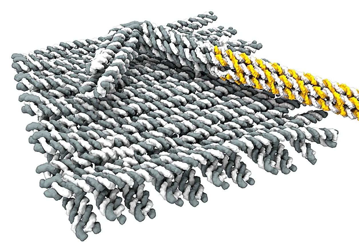
Scientists have engineered a nanoscale switch using DNA “origami.” Inspired by macroscale mechanical switches, the device achieves long-term functionality without the continuous forcing mechanism that past versions required while remaining capable of fast switching. The paper is published in the journal Science Robotics.
This is not the first time scientists have used DNA as a building material. DNA origami—a technique that folds a single-stranded DNA scaffold into precise 2D or 3D shapes using short DNA strands—offers a way to build custom nanomachines. It has been used in everything from drug delivery to electrically actuated devices. However, in electrically actuated devices, many prior designs faced a trade-off between speed, stability and durability.
In particular, researchers have been interested in creating nanoscale switches that act like their macroscopic counterparts. So far, attempts at DNA-based nanoswitches have lacked either long-term stability without continuous forcing, millisecond switching or high cycle endurance. Many earlier devices relied on DNA “latches,” but these were slow or prone to spontaneous dissociation from natural nanoscale thermal movements.

Neuromorphic computing has the potential to overcome limitations of traditional silicon technology in machine learning tasks. Recent advancements in large crossbar arrays and silicon-based asynchronous spiking neural networks have led to promising neuromorphic systems. However, developing compact parallel computing technology for integrating artificial neural networks into traditional hardware remains a challenge. Organic computational materials offer affordable, biocompatible neuromorphic devices with exceptional adjustability and energy-efficient switching. Here, the review investigates the advancements made in the development of organic neuromorphic devices. This review explores resistive switching mechanisms such as interface-regulated filament growth, molecular-electronic dynamics, nanowire-confined filament growth, and vacancy-assisted ion migration, while proposing methodologies to enhance state retention and conductance adjustment. The survey examines the challenges faced in implementing low-power neuromorphic computing, e.g., reducing device size and improving switching time. The review analyses the potential of these materials in adjustable, flexible, and low-power consumption applications, viz. biohybrid spiking circuits interacting with biological systems, systems that respond to specific events, robotics, intelligent agents, neuromorphic computing, neuromorphic bioelectronics, neuroscience, and other applications, and prospects of this technology.
Keywords: Brain-inspired neuromorphic computing; Neuromorphic bioelectronics; Neuroscience; Organic materials; Resistive switching mechanisms.
© 2025. The Author(s).
Endometriosis is a painful, common condition affecting women worldwide, but treatment and diagnosis options are scarce. A new University of Mississippi-led study may have found an answer to both problems.
Early results from a study published in Communications Chemistry show that gold-laced nanoparticles can hitchhike on white blood cells. By using those cells as a delivery vehicle, the team hopes to identify and treat endometriosis without repeated surgeries.
“Lots of women go through their lives being in enormous amounts of pain and thinking that it’s normal, and it’s not normal,” said Eden Tanner, assistant professor of chemistry and biochemistry, who authored the study with a team of Ole Miss researchers.
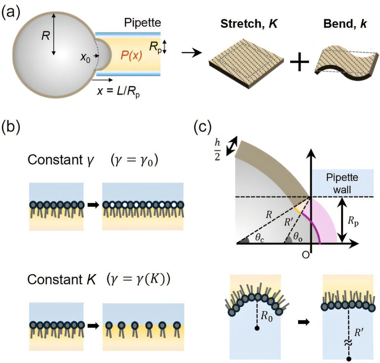
What if the mechanical properties of a cell could be programmed like the components of a machine? Researchers at the University of Tokyo have discovered that two fundamental modes of cellular deformation—stretching and bending—can be independently controlled using different molecular building blocks. The finding provides a new strategy for engineering artificial cells, drug-delivery capsules and adaptive soft materials with precisely tailored mechanical functions.
Miho Yanagisawa, an associate professor at the University of Tokyo, and Kazutoshi Masuda, a Ph.D. student, developed a new framework for dissecting the mechanics of artificial cells. Using lipid-coated microdroplets as simplified cell models, they combined micropipette aspiration experiments with a theoretical model that separates membrane mechanics into stretching and bending contributions. The approach successfully captured nonlinear deformation behaviors that conventional models could not explain. The work is published in the journal Small Science.
The researchers found that lipid molecular geometry primarily determines membrane stretching elasticity. In contrast, when Y-shaped DNA motifs were interconnected to form a three-dimensional network, they created a nanoscale scaffold that dramatically enhanced resistance to bending while leaving stretching elasticity largely unchanged.
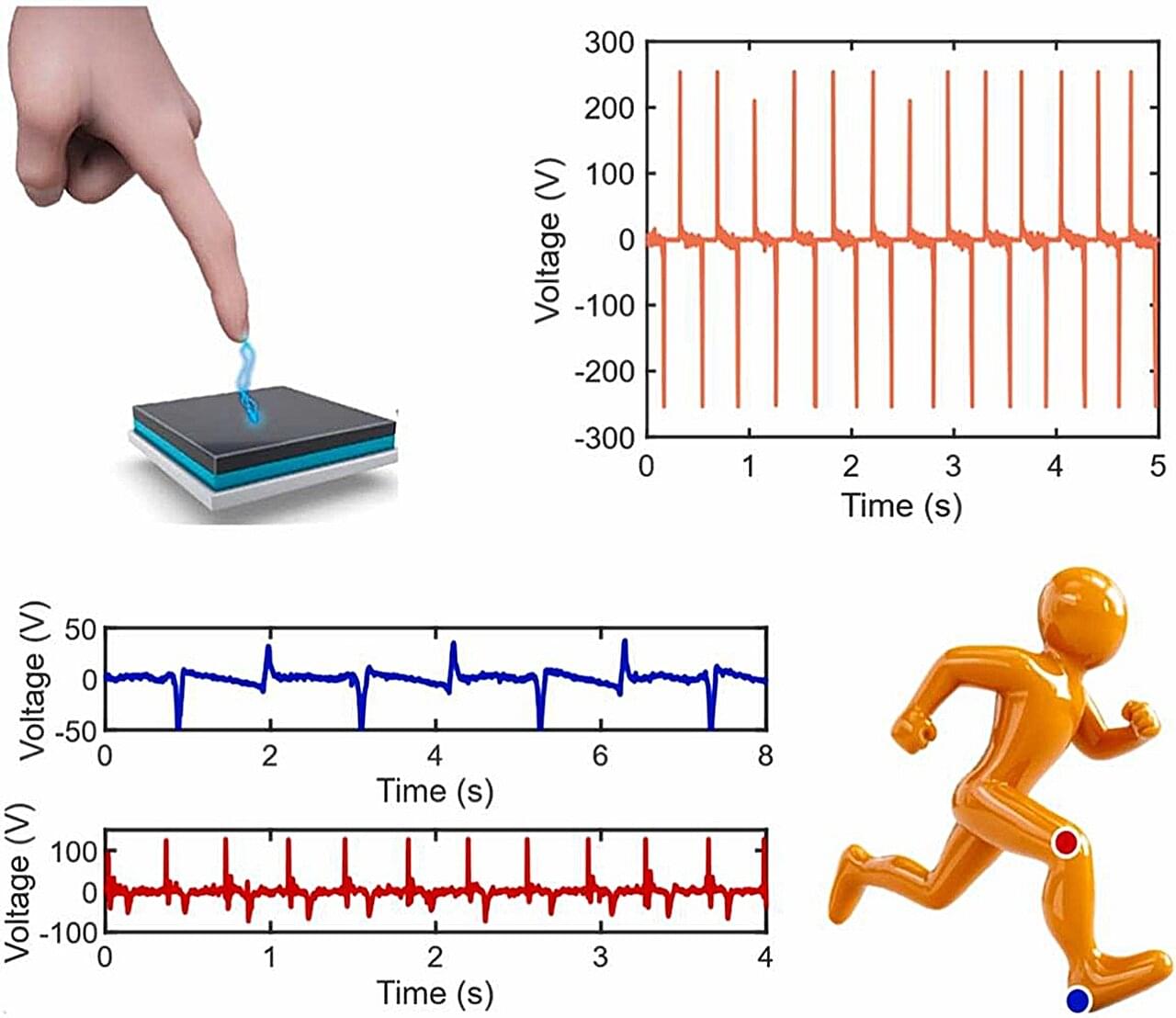
Researchers at Boise State University have developed a novel, environmentally friendly triboelectric nanogenerator (TENG) that is fully printed and capable of harvesting biomechanical and environmental energy while also functioning as a real-time motion sensor. The innovation leverages a composite of Poly (vinyl butyral-co-vinyl alcohol-co-vinyl acetate) (PVBVA) and MXene (Ti3C2Tx) nanosheets, offering a sustainable alternative to conventional TENGs that often rely on fluorinated polymers and complex fabrication.
TENGs are innovative energy-harvesting devices that convert mechanical energy into electricity using the triboelectric effect. They were invented by Prof. Zhong Lin Wang of the Georgia Institute of Technology and generate power through contact and motion between materials, making them ideal for applications like wearable electronics, IoT sensors, and self-powered devices.
This work, published in the journal Nano Energy and led by Ph.D. student Ajay Pratap under the supervision of Prof. David Estrada of the Micron School of Materials Science and Engineering at Boise State University, showcases how additive manufacturing can produce high-performance, skin-compatible, and flexible devices for real-world applications in energy harvesting, wearables electronics, and human-machine interaction.