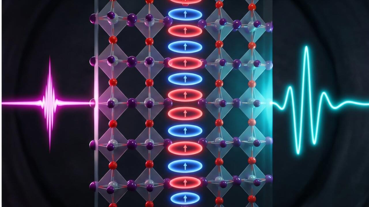
Simulating the nonlinear optical physics that underlies ultrafast laser systems is computationally demanding—a practical bottleneck in settings that require rapid feedback. A study by researchers at Stanford University, University of California, Los Angeles (UCLA), and SLAC National Accelerator Laboratory introduces a deep learning surrogate that delivers orders-of-magnitude acceleration over conventional simulation methods, while maintaining high fidelity across a challenging range of pulse shapes.
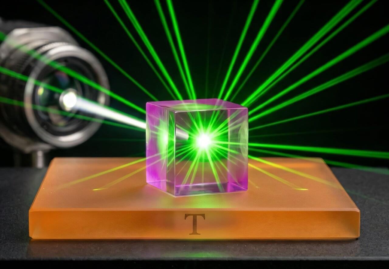
The work centers on second-order nonlinear optics (χ² processes), in which light waves exchange energy inside specially engineered crystals to generate new frequencies and tailored pulse shapes. In particle accelerator facilities, these processes play a key role. At SLAC’s upgraded Linac Coherent Light Source (LCLS-II), infrared laser pulses are first to green light and then to ultraviolet (UV). The UV pulse strikes a cathode to liberate an electron bunch that is subsequently accelerated and modulated to produce intense X-ray pulses. The temporal shape of the UV pulse directly influences the properties of that electron bunch—and ultimately the quality of the X-rays available for science.
A surrogate model for the nonlinear χ² frequency conversion step at the heart of this process is reported in Advanced Photonics.


