Sheaf-ADMM: a different way to build a neural network based on multi-agent consensus, at the intersection of sheaf theory and ADMM for distributed consensus.
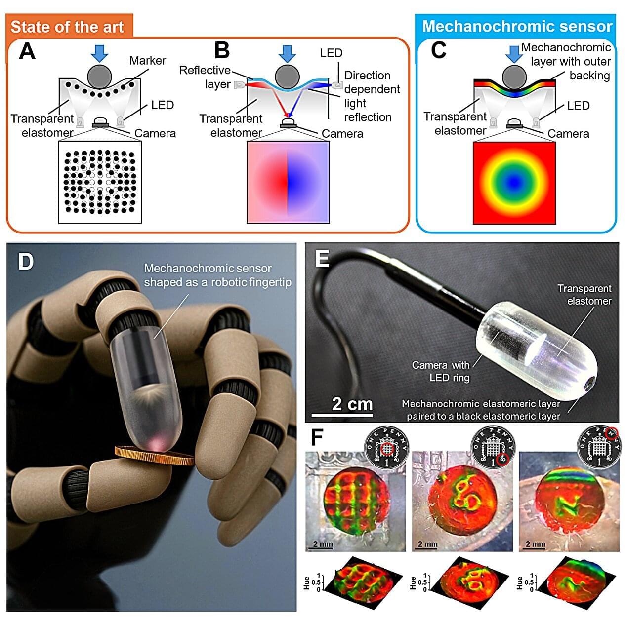
Engineers at Queen Mary University of London have built a new color-changing tactile sensor, which allows robots to “see” and touch in real-time. The novel idea was invented by Giacomo Sasso, a postdoctoral researcher at the School of Engineering and Materials Science at Queen Mary University of London, and it works by transforming invisible forces into dynamic color patterns. This enables high-resolution maps of contact, strain and pressure to emerge instantly.
The study is published in the journal Science Advances.
When pressure is applied to a soft sensing surface, the material produces spatially varying structural colors that can be captured immediately using a standard camera, removing the need for complex reconstruction algorithms.
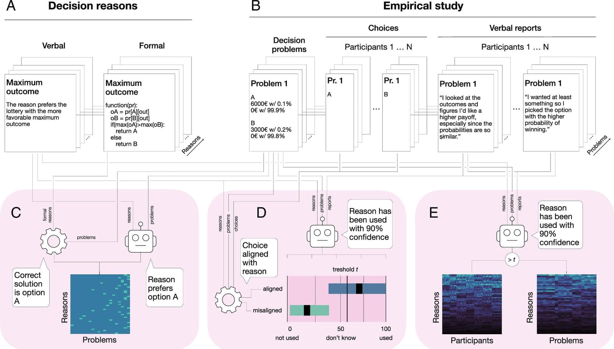
Why do people make the choices they do? Researchers from the Center Synergy of Systems (SynoSys) at TUD Dresden University of Technology, the Max Planck Institute for Human Development, and the University of Basel present their new approach to finding answers to that question. The approach combines observed choices with participants’ own descriptions of their decision processes, allowing researchers to study human behavior in greater detail than is possible with behavioral data alone.
The team merged behavioral experiments and free-text explanations to uncover the reasons underlying human decisions with the help of large language models (LLM). Their results are published in the Proceedings of the National Academy of Sciences.
Machine learning systems sit at the heart of modern AI workloads. In these systems, performance often comes down to the quality of a small number of GPU kernels. Attention kernels, LLM prefill and decode kernels, low-precision block-scaled GEMMs, fused MoE layers, and other large fused kernels all directly shape end-to-end speed in both training and serving.
To make these kernels fast, however, we need more than a list of optimization tricks. Modern GPUs are no longer simple variations of the same old design. Recent architectures introduce richer memory spaces, new access patterns, and increasingly specialized execution units. To program them well, we need both a clear mental model of the hardware and a practical understanding of how high-performance kernels are built. This book is about developing both.
The book follows a simple progression: first understand the GPU hardware, then learn the programming model we will use, and finally build state-of-the-art kernels step by step. Our main target is the Blackwell generation, and our main running examples are General Matrix-Matrix Multiplication (GEMM) and FlashAttention. Along the way, we will also study the core ingredients behind GPU optimization: data layout, asynchronous data movement, and asynchronous coordination.


After 300+ interviews on Singularity. FM, I ended up on the other side of the microphone.
Cadell Last invited me to Philosophy Portal and asked the questions that go all the way down. How a Bulgarian army nickname became “Socrates,” and why it started as an insult. How 300 resumes and one failed job interview accidentally started Singularity Weblog. And why, after 17 years of studying the technological singularity, I believe its biggest prophets got the most important thing wrong.
Ray Kurzweil is a genius and a genuinely humble human being. I’ve interviewed him and spent hours in his office. But his six epochs of the singularity converge into a single storyline where the universe literally wakes up. That is creationism in scientific clothing. It promises the same heaven of immortality and abundance, and it treats humanity as the chosen species.
Silicon Valley’s version is no better: the march of technology is inevitable, unstoppable, and there is nothing you can do about it.
That is not a prediction. That is a prison.
I grew up behind the Iron Curtain in Bulgaria. I watched the same technology build socialism in the East, democracy in the West, and fascism before both. The big choices are never technological. They are ethical, which is to say political.
The barrier between human thought and machine code is officially gone. 🤯
In my last deep dive, we explored “Vibecoding” and how creators are bypassing traditional development bottlenecks using pure vision. But how does AI actually turn your spoken intent into architecture?
AI doesn’t just use a massive translation dictionary. Instead, it operates in a hidden mathematical geometry known as the Latent Space.
In this invisible architecture, an English phrase and a complex Python script are mapped into the exact same coordinate of pure logic. This triggers a massive paradigm shift called Decision Compression—completely erasing the buggy, high-friction “Telephone Game” of traditional software development by binding your raw idea directly to execution.
If AI completely bypasses the need for manual translation, what happens to traditional coding syntax like Java or C++?
And more importantly, who becomes the ultimate builder in this new paradigm?
Read the full deep dive into the engine of the AI revolution!

In 2023, scientists at the Paris Brain Institute investigated one of the most fascinating and unsettling transitions in neuroscience: what happens to the cortex when the brain is deprived of oxygen.
In a rat model of systemic anoxia, researchers found that the dying brain does not simply “shut off” all at once. Instead, cortical activity follows a structured sequence: brief high-frequency activity, slowing oscillations, electrical silence, and then a massive wave of anoxic depolarization — often called the “wave of death.”
This wave appeared to begin deep in the neocortex, especially around layer 5 pyramidal neurons, before spreading upward toward the cortical surface and downward toward the white matter. These neurons are large, metabolically demanding projection cells, which may make them especially vulnerable when oxygen and ATP collapse.
But the most important part of the study is that this wave did not always represent an absolute point of no return. When oxygenation was restored within a critical window, researchers observed a “wave of resuscitation,” followed by partial recovery of synaptic activity.
That does not mean death has been “reversed” in a simple or sensational sense. But it does suggest something scientifically powerful: the boundary between life and death in the brain may be more dynamic, layered, and measurable than we often imagine.
This is where the implications become fascinating.
If the “wave of death” is an organized biophysical event, future neurocritical care may one day be able to detect the brain’s approach toward irreversible injury in real time. Instead of relying only on broad markers like heartbeat, oxygen saturation, or flat EEG, clinicians may eventually use more detailed brain-state monitoring to identify whether the cortex is entering a reversible, borderline, or irreversible phase.
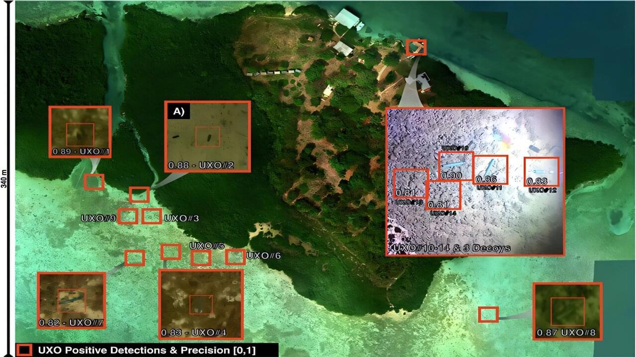
A new airborne imaging approach can reliably detect unexploded weapons that lie in shallow coastal waters and remain an ongoing hazard to public safety, marine ecosystems and infrastructure worldwide. By combining advanced multispectral sensing with artificial intelligence, the researchers were able to identify underwater munitions with high confidence, even when they are partially hidden by sediment, biological growth or debris.
Scientists at the University of Miami Rosenstiel School of Marine, Atmospheric, and Earth Science developed and tested the approach and published their findings in the April issue of Frontiers in Marine Science. The study demonstrates that integrating NASA underwater imaging technologies with machine learning enhances detection accuracy while reducing false positives in complex marine environments.
“Unexploded ordnance in shallow waters remains a serious global challenge,” said Ved Chirayath, Vetlesen Endowed Chair of Earth Sciences in the Department of Ocean Sciences, the study’s lead author. “Our results demonstrate a scalable, airborne solution that can help improve detection accuracy and support safer coastal environments.”
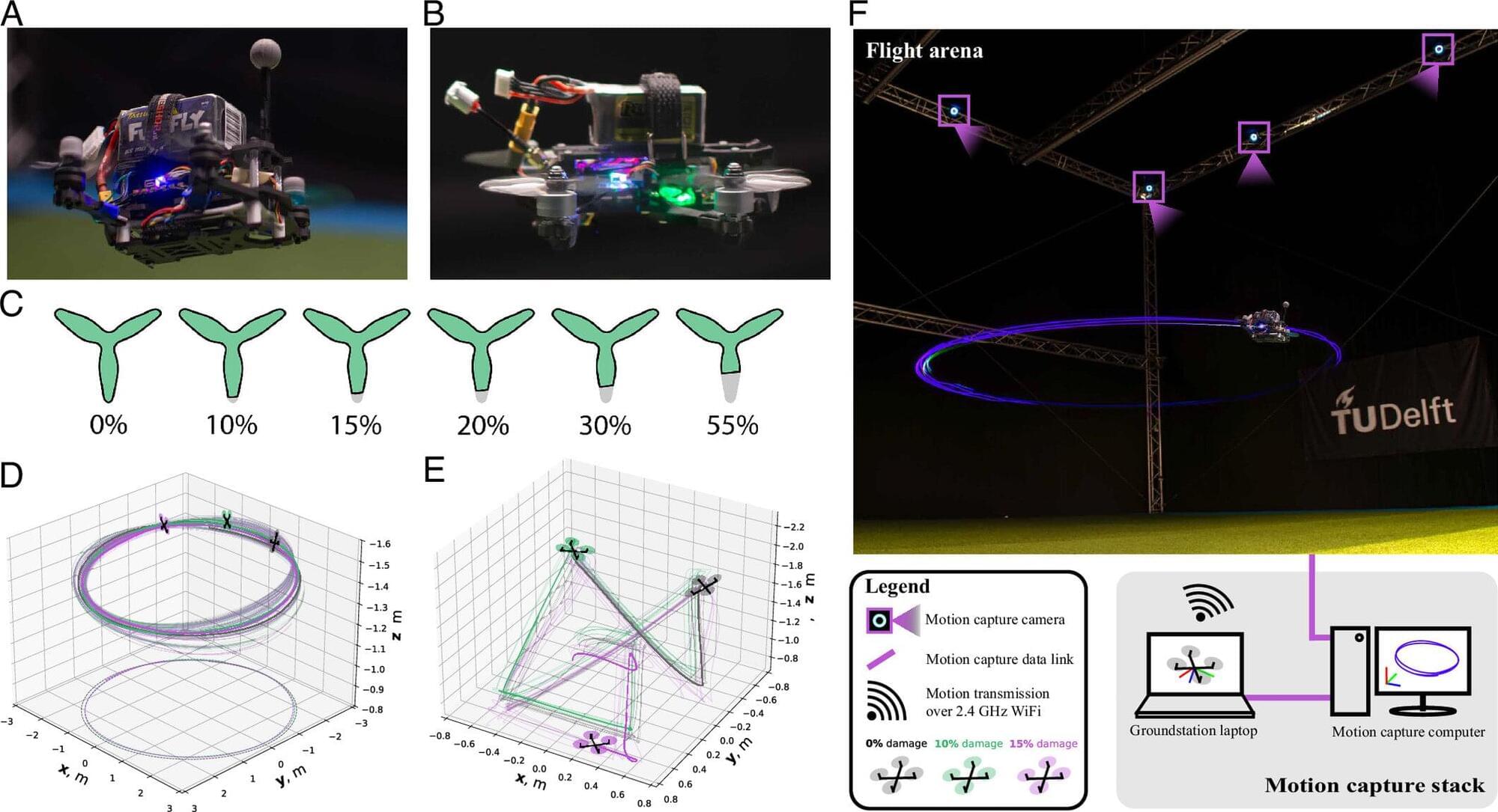
Imagine you’re running and you sprain your ankle. The pain makes you gingerly limp the rest of the way home. This is a great example of how nature adapts to failures in a system. The pain tells you: “If you continue running like normal, the injury will only get worse.” So you naturally adjust the way you run. Drones currently cannot do this with a worn-out propeller.
Researchers from Delft University of Technology and Wageningen University & Research have now demonstrated that a concept we learned from nature, which was originally developed to predict collapse in ecosystems, can also help detect when engineered systems are heading toward failure. This is crucial for ensuring drone and autonomous vehicle safety as they increasingly become part of everyday life.
“You can compare our approach to the way humans experience pain. After an injury, pain provides immediate feedback about our condition and helps us judge what actions remain safe,” says Jasper van Beers, a researcher at Delft University of Technology. “Machines generally lack this form of self-awareness. The new indicators, derived from real-time measurement data, offer a first step toward giving engineered systems a similar ability to recognize when they are approaching their limits.”