Toggle light / dark theme

New nanomagnet production process improves efficiency and cuts costs

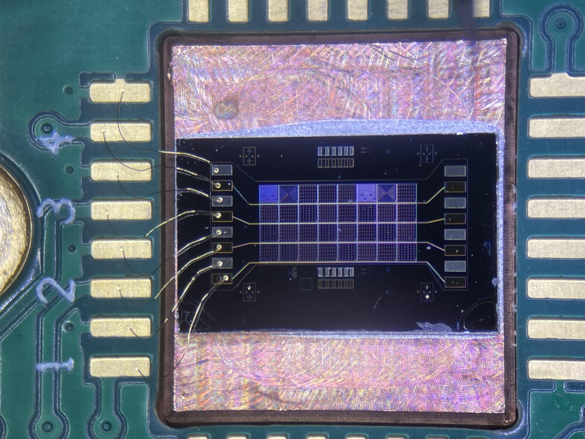
Researchers at HZDR have partnered with the Norwegian University of Science and Technology in Trondheim, and the Institute of Nuclear Physics in the Polish Academy of Sciences to develop a method that facilitates the manufacture of particularly efficient magnetic nanomaterials in a relatively simple process based on inexpensive raw materials.

Using a highly focused ion beam, they imprint magnetic nanostrips consisting of tiny, vertically aligned nanomagnets onto the materials. As the researchers have reported in the journal Advanced Functional Materials, this geometry makes the material highly sensitive to external magnetic fields and current pulses.

Nanomagnets play a key role in modern information technologies. They facilitate fast data storage, precise magnetic sensors, novel developments in spintronics, and, in the future, quantum computing. The foundations of all these applications are functional materials with particular magnetic structures that can be customized on the nanoscale and precisely controlled.

From light to logic: Ultrafast quantum switching in 2D materials

Scientists from the Indian Institute of Technology Bombay have found a way to use light to control and read tiny quantum states inside atom-thin materials. The simple technique could pave the way for computers that are dramatically faster and consume far less power than today’s electronics.

The materials studied are just one atom thick—far thinner than a human hair—and are known as two-dimensional (2D) semiconductors. Inside these materials, electrons can sit in one of two distinct quantum states, called valleys. These valleys, named K and K′, can be thought of as two different “locations” that an electron can choose between. Because there are two options, researchers have long imagined using them like the 0 and 1 of digital computing, but on a quantum level. This idea is the foundation of a rapidly growing research field called valleytronics.

However, being able to reliably control which valley electrons occupy—and to switch between them quickly and on demand—has been a major challenge. “Previous methods required complicated experimental setups with carefully tuned circularly polarized lasers and often multiple laser pulses, and they only worked under specific conditions,” said Prof. Gopal Dixit.

Surprising nanoscopic heat traps found in diamonds

Diamond is famous in material science for being the best natural heat conductor on Earth—but new research reveals that, at the atomic scale, it can briefly trap heat in unexpected ways. The findings could influence how scientists design diamond-based quantum technologies, including ultra-precise sensors and future quantum computers.

In a study published in Physical Review Letters, researchers from the University of Warwick and collaborators showed that when certain molecular-scale defects in diamond are excited with light, they create tiny, short-lived “hot spots” that momentarily distort the surrounding crystal. These distortions last only a few trillionths of a second but are long enough to affect the behavior of quantum-relevant defects.

“Finding a hot ground state for a molecular-scale defect in diamond was extremely surprising for us,” explained Professor James Lloyd-Hughes, Department of Physics, University of Warwick. “Diamond is the best thermal conductor, so one would expect energy transport to prevent any such effect. However, at the nanoscale, some phonons—packets of vibrational energy—hang around near the defect, creating a miniature hot environment that pushes on the defect itself.”

Laser draws made-to-order magnetic landscapes

Researchers at the Paul Scherrer Institute PSI, in collaboration with the National Institute of Standards and Technology (NIST) in Boulder, Colorado, have for the first time succeeded in using existing laser technology to continuously vary the magnetic properties of two-dimensional materials.

This simple and fast method should make a large number of applications possible, including techniques for data storage and processing. The work is published in the journal Nature Communications.

Sometimes using conventional tools in a novel way produces astounding results. That’s what happened when researchers used the high-tech laser equipment in PSI’s cleanroom for something it was not intended to do. It was originally purchased for photolithography—a process for producing tiny 2D structures.

‘Light-bending’ material that controls blue and ultraviolet light could transform advanced chipmaking

Researchers from TU Delft and Radboud University (The Netherlands) have discovered that the two-dimensional ferroelectric material CuInP₂S₆ (CIPS) can be used to control the pathway and properties of blue and ultraviolet light like no other material can.

With ultraviolet light being the workhorse of advanced chipmaking, high-resolution microscopy and next-generation optical communication technologies, improving the on-chip control over such light is vital. As the researchers describe in the journal Advanced Optical Materials, CIPS can be integrated onto chips, opening exciting new avenues for integrated photonics.

The “impossible” LED breakthrough that changes everything

Scientists have unveiled a technique that uses ‘molecular antennas’ to direct electrical energy into insulating nanoparticles. This approach creates a new family of ultra-pure near-infrared LEDs that could be used in medical diagnostics, optical communication systems, and sensitive detectors.

Researchers at the Cavendish Laboratory, University of Cambridge have discovered how to drive electrical current into materials that normally do not conduct, a feat previously thought impossible under normal conditions. By attaching carefully chosen organic molecules that act like tiny antennas, they have built the first light-emitting diodes (LEDs) from insulating nanoparticles. Their work, reported in Nature, points toward a new generation of devices for deep-tissue biomedical imaging and high-speed data transmission.

Reconfigurable platform slows lights for on-chip photonic engineering

Integrated circuits are the brains behind modern electronic devices like computers or smart phones. Traditionally, these circuits—also known as chips—rely on electricity to process data. In recent years, scientists have turned their attention to photonic chips, which perform similar tasks using light instead of electricity to improve speed and energy efficiency.

Electrons stay put in layers of mismatched ‘quantum Legos’

Electrons can be elusive, but Cornell researchers using a new computational method can now account for where they go—or don’t go—in certain layered materials.

Physics and engineering researchers have confirmed that in certain quantum materials, known as “misfits” because their crystal structures don’t align perfectly—picture LEGOs where one layer has a square grid and the other a hexagonal grid—electrons mostly stay in their home layers.

This discovery, important for designing materials with quantum properties including superconductivity, overturns a long-standing assumption. For years, scientists believed that large shifts in energy bands in certain misfit materials meant electrons were physically moving from one layer to the other. But the Cornell researchers have found that chemical bonding between the mismatched layers causes electrons to rearrange in a way that increases the number of high-energy electrons, while few electrons move from one layer to the other.

Quantum Tech Hits Its “Transistor Moment,” Scientists Say

A new article examines the history of computing to help outline the direction of quantum research. It reports that quantum technology is advancing quickly, and that the major obstacles now involve expanding the systems to larger scales. Quantum technology is quickly moving beyond experimental set

/* */