Engineers have invented an ingenious liquid-metal pump that could make future soft robotics and wearable devices much more portable and agile. The innovation, led by the University of Bristol and published in the journal Nature Communications, presents a low-voltage power source with the potential to transform robotic systems for a wide range of applications, from robotic legs to haptic gloves used in medical and industrial settings.
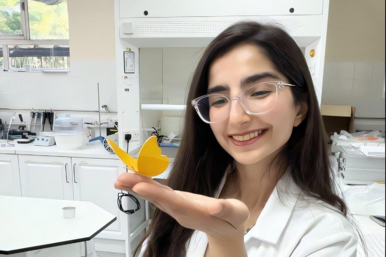
The researchers have demonstrated the varied uses of this innovative technique by creating three prototypes including robotic butterfly wings, a color-changing bracelet, and a haptic fingertip pouch connected to an adjustable wristband which squeezes to simulate natural tactile sensations.w.
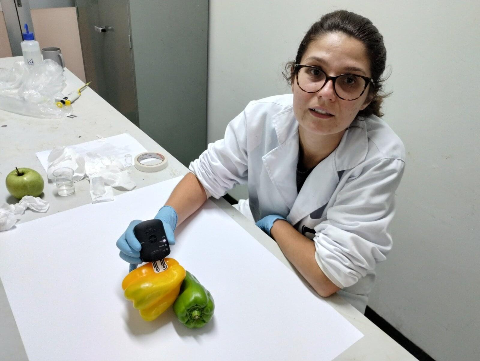
Current technologies are powered by bulky compressors or rigid pumps, which limit mobility and flexibility. The small lightweight soft pump—the size of a pea—is powered by liquid metal, which converts electrical energy into fluid motion, creating an efficient, compact power source for next-generation soft robots and adaptive materials such as medical devices and wearable interfaces for virtual reality.

