There have been a lot of fires in Colorado.
This website uses a security service to protect against malicious bots. This page is displayed while the website verifies you are not a bot.

After 300+ interviews on Singularity. FM, I ended up on the other side of the microphone.
Cadell Last invited me to Philosophy Portal and asked the questions that go all the way down. How a Bulgarian army nickname became “Socrates,” and why it started as an insult. How 300 resumes and one failed job interview accidentally started Singularity Weblog. And why, after 17 years of studying the technological singularity, I believe its biggest prophets got the most important thing wrong.
Ray Kurzweil is a genius and a genuinely humble human being. I’ve interviewed him and spent hours in his office. But his six epochs of the singularity converge into a single storyline where the universe literally wakes up. That is creationism in scientific clothing. It promises the same heaven of immortality and abundance, and it treats humanity as the chosen species.
Silicon Valley’s version is no better: the march of technology is inevitable, unstoppable, and there is nothing you can do about it.
That is not a prediction. That is a prison.
I grew up behind the Iron Curtain in Bulgaria. I watched the same technology build socialism in the East, democracy in the West, and fascism before both. The big choices are never technological. They are ethical, which is to say political.
The barrier between human thought and machine code is officially gone. 🤯
In my last deep dive, we explored “Vibecoding” and how creators are bypassing traditional development bottlenecks using pure vision. But how does AI actually turn your spoken intent into architecture?
AI doesn’t just use a massive translation dictionary. Instead, it operates in a hidden mathematical geometry known as the Latent Space.
In this invisible architecture, an English phrase and a complex Python script are mapped into the exact same coordinate of pure logic. This triggers a massive paradigm shift called Decision Compression—completely erasing the buggy, high-friction “Telephone Game” of traditional software development by binding your raw idea directly to execution.
If AI completely bypasses the need for manual translation, what happens to traditional coding syntax like Java or C++?
And more importantly, who becomes the ultimate builder in this new paradigm?
Read the full deep dive into the engine of the AI revolution!
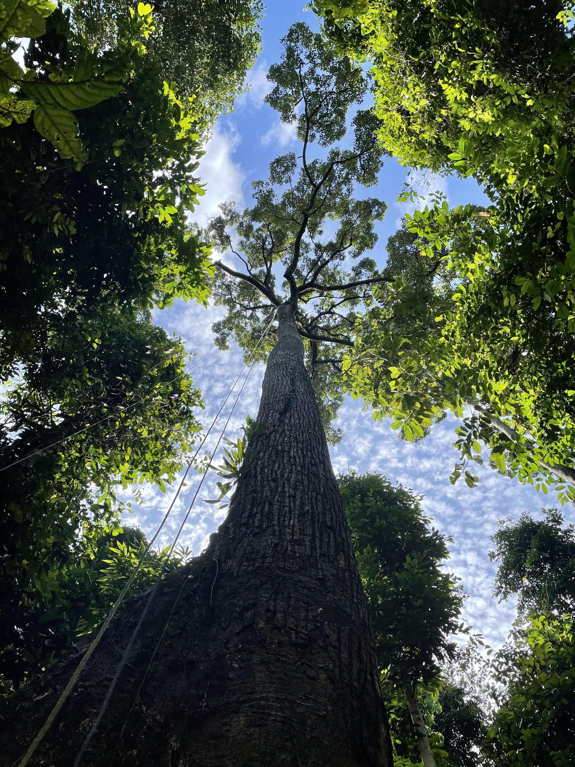
The giant trees of tropical forests are important allies in the fight against climate change because of their ability to store carbon, yet they are still poorly understood by science. However, a study published in the journal Science reveals a crucial survival mechanism: These trees, which exceed 70 meters (230 feet) in height, have no difficulty transporting water to their tops and are no more vulnerable than smaller trees.
They have developed internal adaptations that compensate for the challenges of transporting water to the highest branches. Furthermore, tests conducted during severe droughts showed that they did not experience a more pronounced decline in growth than smaller trees. This contradicts the hypothesis that very tall trees would be more susceptible to water stress.
Nanoparticles are widely used in medicine to deliver drugs, genes or imaging agents to specific parts of the body. Once a nanoparticle reaches a cell, however, many things can happen—it can reach its target, be degraded, interact with proteins that help transport it, or interact with proteins that hinder its transport.
A longstanding problem in designing nanomedicines has been understanding what happens to nanoparticles at the cellular level, but scientists have faced many challenges. For example, optical microscopy imaging techniques provide only a generalized view of nanomedicine localization.
On the other hand, proteomics approaches require cell lysis, which disrupts the natural distribution of proteins around the nanoparticle, making it difficult to understand how nanoparticles are transported within the cell. Another method—proximity labeling—enables in situ investigation of intracellular protein-protein interactions, but it relies on genetically engineered enzyme fusion, which limits its applicability across diverse systems.

A new type of hip replacement implant reduces the risk of joint dislocation after surgery by 70%, according to a new study involving 1,600 patients across 44 hospitals in Sweden and the UK, published in The Lancet. The new implant consists of a small ball encased in a much larger plastic ball, which provides better stability.
Each year, more than 14 million patients worldwide suffer a femoral neck fracture. Total hip replacement (THR), in which both the ball and socket of the hip are replaced, is recommended for older, active individuals with a displaced fracture of the femoral neck. While the vast majority regain good mobility and quality of life, up to 8% of these patients experience a dislocation of their hip, a very painful condition in which the artificial joint slips out of place.

In 2023, scientists at the Paris Brain Institute investigated one of the most fascinating and unsettling transitions in neuroscience: what happens to the cortex when the brain is deprived of oxygen.
In a rat model of systemic anoxia, researchers found that the dying brain does not simply “shut off” all at once. Instead, cortical activity follows a structured sequence: brief high-frequency activity, slowing oscillations, electrical silence, and then a massive wave of anoxic depolarization — often called the “wave of death.”
This wave appeared to begin deep in the neocortex, especially around layer 5 pyramidal neurons, before spreading upward toward the cortical surface and downward toward the white matter. These neurons are large, metabolically demanding projection cells, which may make them especially vulnerable when oxygen and ATP collapse.
But the most important part of the study is that this wave did not always represent an absolute point of no return. When oxygenation was restored within a critical window, researchers observed a “wave of resuscitation,” followed by partial recovery of synaptic activity.
That does not mean death has been “reversed” in a simple or sensational sense. But it does suggest something scientifically powerful: the boundary between life and death in the brain may be more dynamic, layered, and measurable than we often imagine.
This is where the implications become fascinating.
If the “wave of death” is an organized biophysical event, future neurocritical care may one day be able to detect the brain’s approach toward irreversible injury in real time. Instead of relying only on broad markers like heartbeat, oxygen saturation, or flat EEG, clinicians may eventually use more detailed brain-state monitoring to identify whether the cortex is entering a reversible, borderline, or irreversible phase.
“The Commission considers that at this stage it cannot propose a legal obligation to keep videogames playable after they stop being provided commercially. This is due, also, to existing intellectual property rights. Under EU copyright law, rights holders enjoy exclusive rights over their creations.”
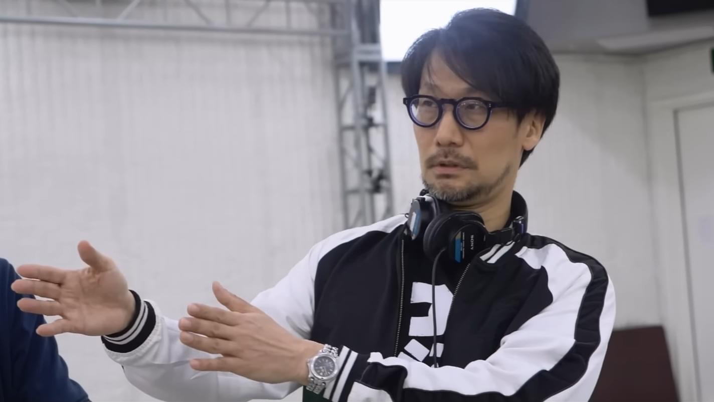
Players are (quite rightly) worried that without physical media their beloved games, or any kind of art, can be ripped away from them at a moment’s notice. “We will not be able to freely access the movies, books, and music that we have loved,” Kojima adds. “I would be a have-not. That’s what I’m afraid of. This is not greed.”