What exists at the core of a black hole? A research team led by Enrico Rinaldi, a physicist at the University of Michigan, has leveraged quantum computing and machine learning to analyze the quantum state of a matrix model, providing new insights into the nature of black holes.
The study builds on the holographic principle, which suggests that the fundamental theories of particle physics and gravity are mathematically equivalent, despite being formulated in different dimensions.
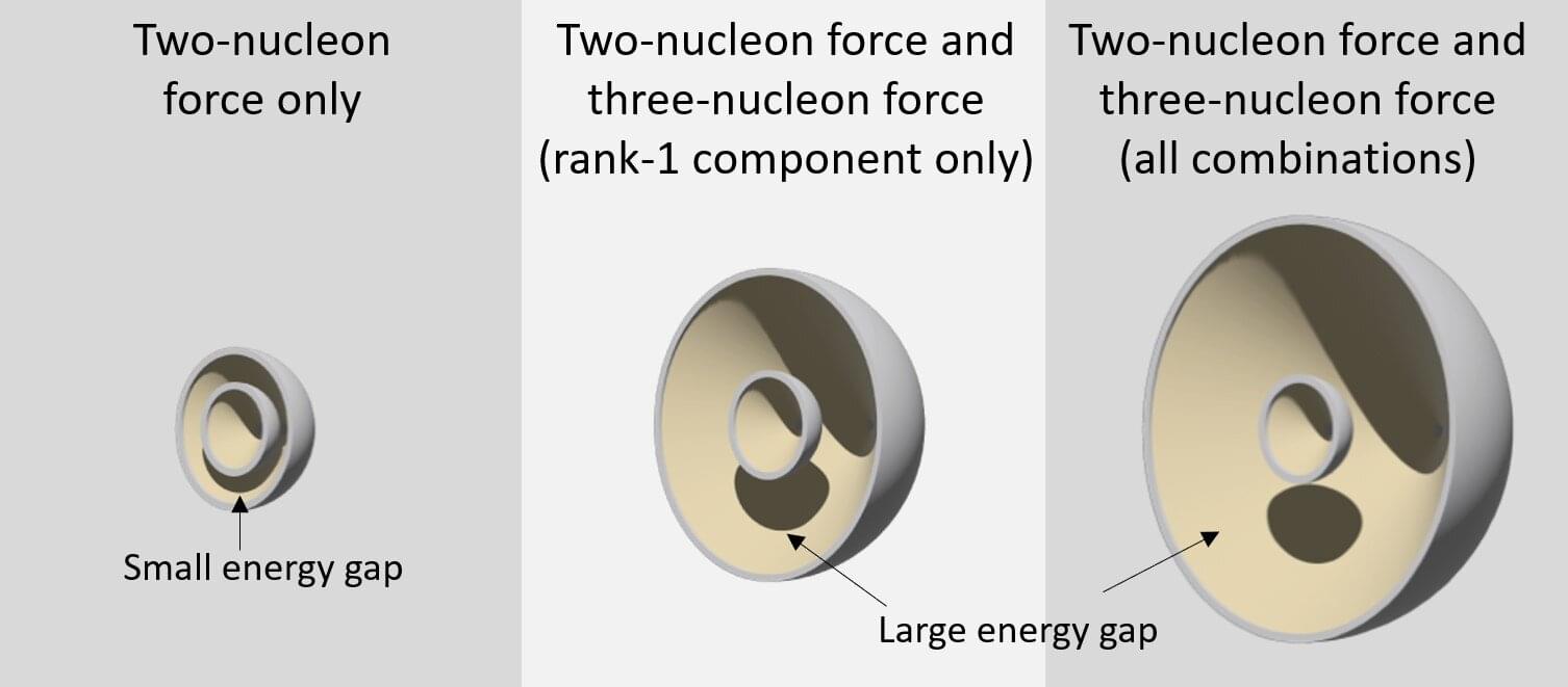
Two prevailing theories describe black holes from different dimensional perspectives. In one framework, gravity operates within the three-dimensional geometry of the black hole. In contrast, particle physics is confined to the two-dimensional surface, resembling a flat disk. This duality highlights a key distinction between the two models while reinforcing their interconnected nature.

