There’s just one catch: every atom in your body would be fully disassembled to the quantum level, effectively leaving your original body totally destroyed.


When lightning strikes, the electrons come pouring down.
In a new study, researchers at CU Boulder led by an undergraduate student have discovered a new link between weather on Earth and weather in space. The group used satellite data to show that lightning storms on our planet can knock especially high-energy, or “extra-hot,” electrons out of the inner radiation belt—a region of space filled with charged particles that surrounds Earth like an inner tube.
The team’s results could help satellites and even astronauts avoid dangerous radiation in space. This is one kind of downpour you don’t want to get caught in, said lead author Max Feinland.

Researchers at the Large Hadron Collider (LHC), the world’s largest particle accelerator, have recently made a groundbreaking advancement in exploring the laws of nature. They have observed the phenomenon of quantum entanglement between top quarks, the heaviest elementary particles, at unprecedented energy levels. This breakthrough paves the way for new possibilities in particle physics and could unveil new aspects of the fundamental forces that govern the universe.
Quantum Entanglement: A Counterintuitive Phenomenon
Quantum entanglement is one of the most enigmatic phenomena in quantum mechanics. It occurs when two or more particles become interconnected in such a way that the state of one particle instantly influences another, regardless of the distance separating them. This defies our everyday intuition and challenges some classical physics concepts, like causality.

Two researchers at The University of Alabama in Huntsville (UAH) have published a paper that demonstrates for the first time that a subluminal warp drive is possible within the bounds of known physics without the need to employ exotic unknown forms of matter or energy, while also advancing our understanding of gravity. UAH alumnus Dr. Jared Fuchs led a team of physicists that produced the paper, supported by Dr. Christopher Helmerich, also an alumnus of UAH, a part of the University of Alabama System, both working in conjunction with the New York-based Applied Propulsion Laboratory of Applied Physics (APL).
When Mexican physicist Miguel Alcubierre first proposed his theoretical warp drive in 1994, the concept required a bubble of ‘negative energy density’ around an object to create an imbalance in space-time, generating motion without movement of the craft, thus avoiding violations of the speed-of-light limit. But the Star Trek dream comes with a catch: it would have to be powered by either exotic particles that haven’t yet been discovered, or the mysterious dark energy thought to drive the expansion of the universe, currently viewed by most physicists as not remotely achievable.
Fuch’s team’s Constant-Velocity Subluminal Warp Drive, however, offers a new means of propulsion that allows it to operate at constant subluminal speeds, while still conforming to Einstein’s theory of general relativity, with no need for ‘unphysical’ forms of matter required by previous designs.


“We can now see the moment where atomic nuclei and electrons are uniting in the afterglow,” team member Rasmus Damgaard, a researcher at the Cosmic DAWN Center, said in a statement. For the first time, we see the creation of atoms, we can measure the temperature of the matter, and we can see the microphysics in this remote explosion.”
“It is like admiring three cosmic background radiation surrounding us from all sides, but here, we get to see everything from the outside. We see before, during, and after the moment of birth of the atoms.”
Neutron stars are born when stars at least 8 times as massive as the sun exhaust their fuel for nuclear fusion and can no longer support themselves against their own gravity.

Inside a hunk of a material called a semimetal, scientists have uncovered signatures of bizarre particles that sometimes move like they have no mass, but at other times move just like a very massive particle.

In a new study, an international team of physicists has unified two distinct descriptions of atomic nuclei, taking a major step forward in our understanding of nuclear structure and strong interactions. For the first time, the particle physics perspective – where nuclei are seen as made up of quarks and gluons – has been combined with the traditional nuclear physics view that treats nuclei as collections of interacting nucleons (protons and neutrons). This innovative hybrid approach provides fresh insights into short-range correlated (SRC) nucleon pairs – which are fleeting interactions where two nucleons come exceptionally close and engage in strong interactions for mere femtoseconds. Although these interactions play a crucial role in the structure of nuclei, they have been notoriously difficult to describe theoretically.
\r \r.
“Nuclei (such as gold and lead) are not just a ‘bag of non-interacting protons and neutrons’,” explains Fredrick Olness at Southern Methodist University in the US, who is part of the international team. “When we put 208 protons and neutrons together to make a lead nucleus, they interact via the strong interaction force with their nearest neighbours; specifically, those neighbours within a ‘short range.’ These short-range interactions/correlations modify the composition of the nucleus and are a manifestation of the strong interaction force. An improved understanding of these correlations can provide new insights into both the properties of nuclei and the strong interaction force.”

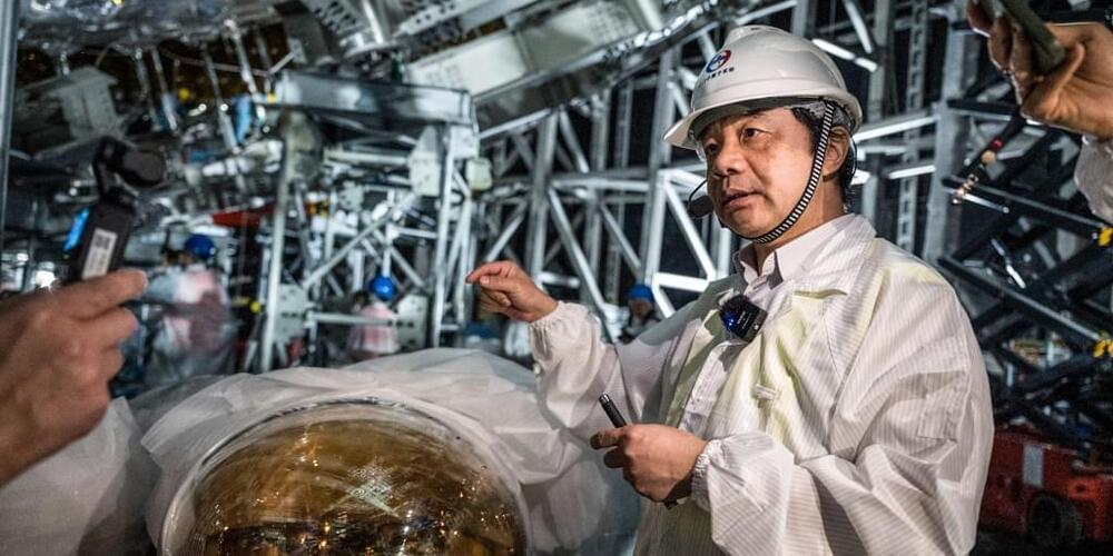
GOLDEN ROOSTER TOWN, Kaiping, China — In a granite cavern deep beneath the forested hills of southern China, workers will soon complete a 600-ton sphere that could crack open some of the deepest mysteries of modern physics.
The plexiglass sphere is the centerpiece of the Jiangmen Underground Neutrino Observatory, or JUNO, a $300 million facility designed to measure neutrinos, the smallest subatomic particles known to physicists.