Nanoscale imaging and control of altermagnetism in manganese telluride is achieved, paving the way for the experimental realization of the theoretically predicted field of altermagnetism.
Nanoscale imaging and control of altermagnetism in manganese telluride is achieved, paving the way for the experimental realization of the theoretically predicted field of altermagnetism.
Posted in mobile phones, nanotechnology, particle physics | Leave a Comment on Researchers develop full-color-emitting upconversion nanoparticle technology for ultra-high RGB display quality
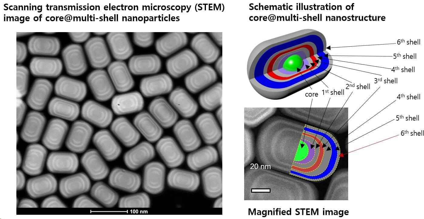
Dr. Ho Seong Jang and colleagues at the Extreme Materials Research Center at the Korea Institute of Science and Technology (KIST) have developed an upconversion nanoparticle technology that introduces a core@multi-shell nanostructure, a multilayer structure in which multiple layers of shells surround a central core particle, and enables high color purity RGB light emission from a single nanoparticle by adjusting the infrared wavelength.
The work is published in the journal Advanced Functional Materials.
Luminescent materials are materials that light up on their own and are used in a variety of display devices, including TVs, tablets, monitors, and smartphones, to allow us to view a variety of images and videos. However, conventional two-dimensional flat displays cannot fully convey the three-dimensional dimensionality of the real world, limiting the sense of depth.
The manufacturing and deployment of hybrid and electric vehicles is on the rise, contributing to ongoing efforts to decarbonize the transport industry. While cars and smaller vehicles can be powered using lithium batteries, electrifying heavy-duty vehicles, such as trucks and large buses, has so far proved much more challenging.
Fuel cells, devices that generate electricity via chemical reactions, are promising solutions for powering heavy-duty vehicles. Most of the fuel cells employed so far are so-called proton exchange membrane fuel cells (PEMFCs), cells that generate electricity via the reaction of hydrogen and oxygen, conducting protons from their anode to their cathode utilizing a solid polymer membrane.
Despite their potential, many existing fuel cells have limited lifetimes and efficiencies. These limitations have so far hindered their widespread adoption in the manufacturing of electric or hybrid trucks, buses and other heavy-truck vehicles.

As the demand for innovative materials continues to grow—particularly in response to today’s technological and environmental challenges—research into nanomaterials is emerging as a strategic field. Among these materials, quantum dots are attracting particular attention due to their unique properties and wide range of applications. A team of researchers from ULiège has recently made a significant contribution by proposing a more sustainable approach to the production of these nanostructures.
Quantum dots (QDs) are nanometer-sized semiconductor particles with unique optical and electronic properties. Their ability to absorb and emit light with high precision makes them ideal for use in solar cells, LEDs, medical imaging, and sensors.
In a recent study, researchers at ULiège developed the first intensified, scalable process to produce cadmium chalcogenide quantum dots (semiconducting compounds widely used in optoelectronics and nanotechnology) in water using a novel, biocompatible chalcogenide source (chemical elements such as sulfur, selenium, and tellurium).
Technology for converting solar energy into thermal energy is ever evolving and has numerous applications. A breakthrough in the laboratory of Professor My Ali El Khakani at Institut national de la recherche scientifique (INRS) has made a significant contribution to the field.
Professor El Khakani specializes in plasma-laser processes for the development of nanostructured materials. He and his team at the Énergie Matériaux Télécommunications Research Center have developed a new photothermal material that converts sunlight into heat with unmatched efficiency. The results of their work were published in the journal Scientific Reports.
For several decades, stoichiometric titanium oxides have been known for their exceptional photocatalytic properties. A sub-stoichiometric form of this material, characterized by a slight deficiency in oxygen atoms, is referred to as “Magnéli phases,” with specific compositions exhibiting distinct properties.
A simple tweak to the usual setup is all that is needed to enhance a spectroscopy technique that uses waves in the terahertz region to probe samples, RIKEN physicists have discovered. The findings are published in the journal Applied Physics Letters.
Developing techniques that can obtain spectra from tiny regions extremely rapidly is the ultimate goal of a team that Norihiko Hayazawa of the RIKEN Center for Advanced Photonics belongs to.
Until recently, the scientists had been focusing on obtaining spectra from nanoscale regions on samples. But now they are concentrating on acquiring spectra very quickly—on the order of billionths of seconds (nanoseconds)—to minimize fluctuations induced by the ambient environment.

A study from Technion unveils a newly discovered form of quantum entanglement in the total angular momentum of photons confined in nanoscale structures. This discovery could play a key role in the future miniaturization of quantum communication and computing components.
Quantum physics sometimes leads to very unconventional predictions. This is what happened when Albert Einstein and his colleagues, Boris Podolsky and Nathan Rosen (who later founded the Faculty of Physics at Technion), found a scenario in which knowing the state of one particle immediately affects the state of the other particle, no matter how great the distance between them. Their historic 1935 paper was nicknamed EPR after its three authors (Einstein–Podolsky–Rosen).
The idea that knowing the state of one particle will affect another particle located at a huge distance from it, without physical interaction and information transfer, seemed absurd to Einstein, who called it “spooky action at a distance.”
The same unique structure that makes plastic so versatile also makes it susceptible to breaking down into harmful micro- and nanoscale particles. The world is saturated with trillions of microscopic and nanoscopic plastic particles, some smaller than a virus, making them small enough to interfere
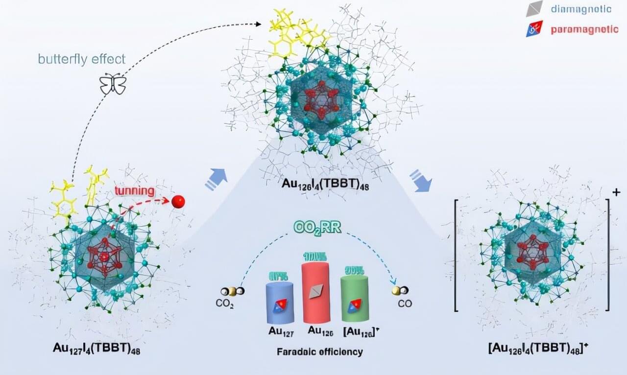
Recently, a team of researchers from the Hefei Institutes of Physical Science of the Chinese Academy of Sciences (CAS) consecutively removed the innermost atom and the outermost electron of a gold nanoparticle—without disturbing its overall structure. This precise manipulation allowed them to probe how the magnetic spin of the material influences its catalytic activity.
The work, led by Prof. Wu Zhikun in collaboration with Prof. Yang from the Institute of Process Engineering, CAS and Prof. Tang from Chongqing University, was published in Science Advances.
Gold nanoclusters—tiny particles composed of from a few to hundreds of gold atoms —are ideal models for studying how atomic structure affects material properties. But tuning the structure of such clusters atom by atom, especially when they’re relatively large and complex, has long been a major challenge.
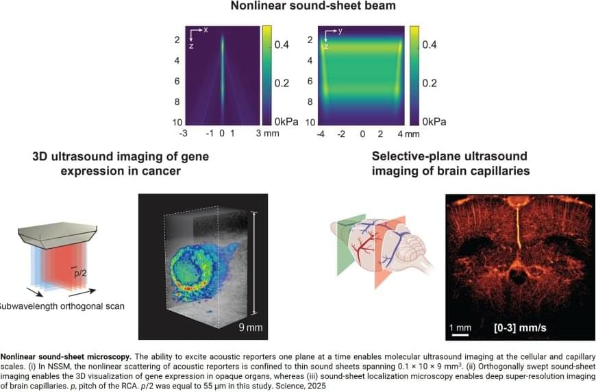
Key to this innovation in ultrasound imaging—a method called Nonlinear sound sheet microscopy —was the discovery of a sound-reflecting probe. The author said: “This probe is a nanoscale gas-filled vesicle that lights up in ultrasound images, making cells visible. These vesicles have a protein shell and we can engineer them to tune their brightness in images. We used these gas vesicles to track cancer cells.”
In addition to revealing cells, the team used ultrasound and microbubbles as probes circulating in the blood stream to detect brain capillaries. The author said: “To our knowledge, nonlinear sound sheet microscopy is the first technique capable of observing capillaries in living brains. This breakthrough has tremendous potential to diagnose small vessel diseases in patients.” Since microbubble probes are already approved for human use, this technique could be deployed in hospitals in a few years.
Ultrasound is one of the most widely used imaging techniques in medicine, but up until recently it hardly played a role in imaging the tiniest structures of our bodies such as cells. “Clinical ultrasound, like the kind used for pregnancy scans, creates real-time images of body parts”, the first author explains. “It allows diagnosis of various diseases, or to monitor a developing baby. However, what is going on at a microscopic level remains hidden.”
Now, a team of scientists managed to image specifically labelled cells in 3D with ultrasound. For the first time, they imaged living cells inside whole organs across volumes the size of a sugar cube. In comparison, current light-based microscopes often require imaging of non-living samples, the author says. “The sample or organ of interest has to be removed and processed, and you lose the ability to track activity of cells over time”