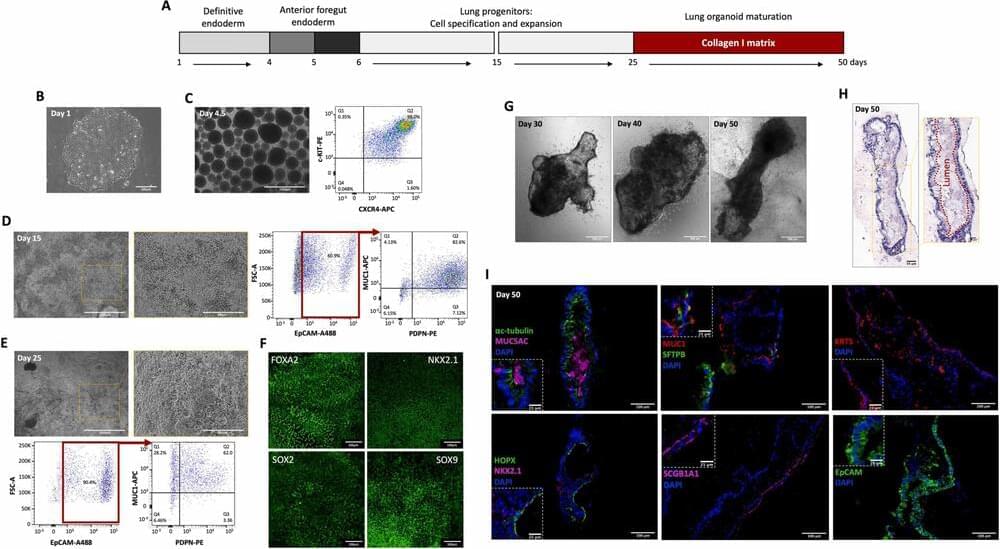
Human mini-lungs grown by University of Manchester scientists can mimic the response of animals when exposed to certain nanomaterials. The study is published in Nano Today.

T-Cell Priming Immunotherapies To Provide Broad And Robust, Long-Term Immunity — Prof. Dr. Thomas Rademacher, MD, PhD — CEO & Co-Founder, Emergex Vaccines
Professor Dr. Thomas Rademacher, MD, PhD, is CEO and Co-Founder of Emergex (https://emergexvaccines.com/), a company that has developed a novel nanoparticle-based vaccine technology to deliver synthetic viral fragments via microneedles on a skin-adhesive patch. Emergex’s approach works on the principle of priming immune T-cells, opening the door for the development of universal vaccines against highly mutagenic viruses such as the seasonal flu and covid. T-cell priming offers a superior inoculation strategy over traditional vaccines, which rely on the body’s generation of antibodies and fail to keep up with seasonal mutations.
A serial entrepreneur, Professor Rademacher also serves as Emeritus Professor of Molecular Medicine at University College London (UCL) and is widely considered one of the founders of biotech from the early 1980s (having been involved in many of it’s core disciplines – from recombinant proteins, to monoclonal antibodies, to glycobiology).
Professor Rademacher has authored over 200 publications and 50 patents – 19 of which are in the nanomedicine field. In addition to being a world leader in nanomedicine, he is also an expert in fetal-maternal medicine, having produced 25 publications and filed 5 patents related to preeclampsia.
Professor Rademacher was co-Founder of the field of Glycobiology and subsequent Glycobiology Institute in Oxford and co-founded Oxford GlycoSciences, the first of Oxford University’s biotech spinouts, which, in 1998, was listed on the London Stock Exchange and reached a market capitalization of £1.7 billion. After moving to UCL, Professor Rademacher founded several biotech spin-out companies, including Rodaris Pharmaceuticals Ltd.

Evan A. Scott, PhD, comes to UVA from Northwestern University, where he has conducted groundbreaking research into the use of tiny nanostructures to battle heart disease, cancer, glaucoma and more. Scott’s nanostructures, far too small for the eye to see, allow for the precise delivery of drugs and other therapeutics to specific inflammatory cells to benefit the body’s immune response. His research provides important answers about the fundamental processes responsible for diseases and paves the way for high-tech treatments using cleverly designed, and mind-blowingly miniscule, synthetic materials.
“We are excited to welcome Dr. Scott to head up nanoSTAR at this critical turning point in nanotechnology research at the University of Virginia,” said Melina R. Kibbe, MD, dean of the School of Medicine. “Nanotechnology has vast untapped potential to benefit patients everywhere. It is a long-standing strength for UVA and will be a foundational pillar of the Paul and Diane Manning Institute of Biotechnology.”
The Manning Institute, under construction at Fontaine Research Park, will tackle some of the greatest challenges in medicine by focusing on cutting-edge areas of research such as nanotechnology, targeted drug delivery, cellular therapies and gene therapy. NanoSTAR, with Scott at the helm, will play a key role in that nanotechnology research, and Scott will work to foster collaborations across Grounds, including among the School of Medicine, School of Engineering and Applied Science, School of Data Science and the College of Arts and Sciences, among others.
Is it possible for nanoparticles to go through the digestive system and deliver medicine directly to the brain tissue? Researchers from Michigan State University say yes, and their latest findings are expected to benefit patients with neurodegenerative disorders like multiple sclerosis, or MS; amyotrophic lateral sclerosis, or ALS; and Parkinson’s disease, or PD.

Researchers have shown that double-layer graphene can function both as a superconductor and an insulator, a property that could revolutionize transistor technology. This dual functionality allows for the development of nanoscale transistors that are highly energy-efficient.
An international research team led by the University of Göttingen has demonstrated experimentally that electrons in naturally occurring double-layer graphene move like particles without any mass, in the same way that light travels. Furthermore, they have shown that the current can be “switched” on and off, which has potential for developing tiny, energy-efficient transistors – like the light switch in your house but at a nanoscale. The Massachusetts Institute of Technology (MIT), USA, and the National Institute for Materials Science (NIMS), Japan, were also involved in the research. The results were published in the scientific journal Nature Communications.

An international research team led by the University of Göttingen has demonstrated experimentally that electrons in naturally occurring double-layer graphene move like particles without any mass, in the same way that light travels.
Furthermore, they have shown that the current can be “switched” on and off, which has potential for developing tiny, energy-efficient transistors – like the light switch in your house but at a nanoscale.
The Massachusetts Institute of Technology (MIT), USA, and the National Institute for Materials Science (NIMS), Japan, were also involved in the research. The results were published in Nature Communications (“Probing the tunable multi-cone band structure in Bernal bilayer graphene”).
It is a common hack to stretch a balloon out to make it easier to inflate. When the balloon stretches, the width crosswise shrinks to the size of a string. Noah Stocek, a Ph.D. student collaborating with Western physicist Giovanni Fanchini, has developed a new nanomaterial that demonstrates the opposite of this phenomenon.
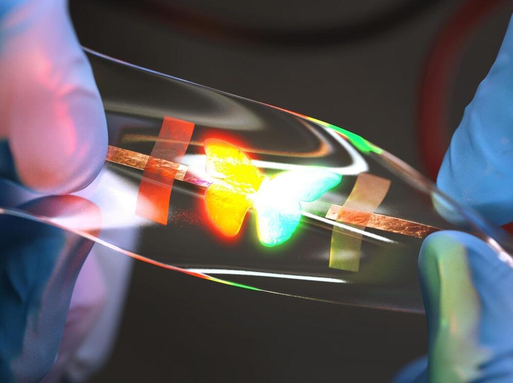
Intrinsically stretchable quantum dot light-emitting diodes. Credit: Institute for Basic Science.
Intrinsically stretchable quantum dot-based light-emitting diodes achieved record-breaking performance.
A team of South Korean scientists led by Professor KIM Dae-Hyeong of the Center for Nanoparticle Research within the Institute for Basic Science has pioneered a novel approach to stretchable displays. The team announced the first development of intrinsically stretchable quantum dot light-emitting diodes (QLEDs).

Study shows neutrons can bind to nanoscale atomic clusters known as quantum dots. The finding may provide insights into material properties and quantum effects.
Neutrons are subatomic particles that have no electric charge, unlike protons and electrons. That means that while the electromagnetic force is responsible for most of the interactions between radiation and materials, neutrons are essentially immune to that force.
Neutron interaction through the strong force.