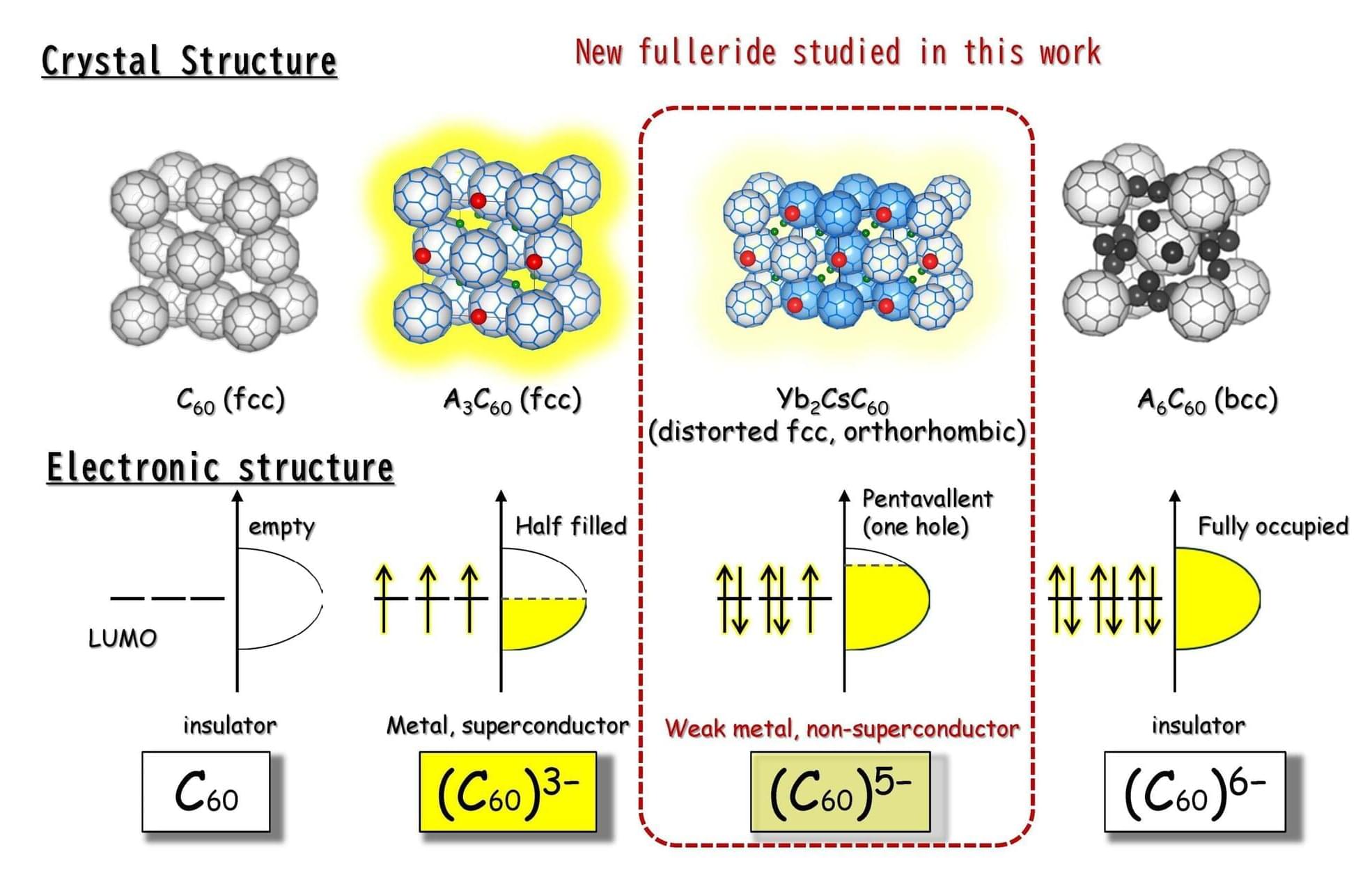
Toggle light / dark theme

All-optical modulation in silicon achieved via an electron avalanche process

Over the past decades, engineers have introduced numerous technologies that rely on light and its underlying characteristics. These include photonic and quantum systems that could advance imaging, communication and information processing.

A key challenge that has so far limited the performance of these new technologies is that most materials used to fabricate them have a weak optical nonlinearity. This essentially means that they do not strongly change in response to light of different intensities.

A strong optical linearity is of crucial importance for the development of ultrafast optical switches, devices that can control either light or electrical signals by modulating the properties of a light-based signal (e.g. its intensity or path). Notably, these switches are central components of fiber optics-based communication systems, photonic devices and quantum technologies.

Colloidal quantum dot photodiodes integrated on metasurfaces for compact SWIR sensors

This week, at the IEEE International Electron Devices Meeting (IEDM 2025), imec, a research and innovation hub in advanced semiconductor technologies, successfully demonstrated the integration of colloidal quantum dot photodiodes (QDPDs) on metasurfaces developed on its 300 mm CMOS pilot line. This pioneering approach enables a scalable platform for the development of compact, miniaturized shortwave infrared (SWIR) spectral sensors, setting a new standard for cost-effective and high-resolution spectral imaging solutions.

Short-wave infrared (SWIR) sensors offer unique capabilities. By detecting wavelengths beyond the visible spectrum, they can reveal contrasts and features invisible to the human eye and can therefore see through certain materials such as plastics or fabrics, or challenging conditions like haze and smoke. Conventional SWIR sensors remain, however, expensive, bulky, and challenging to manufacture, restricting their use to niche applications.

Quantum dot (QD) image sensors, a new class of SWIR sensors, offer a promising alternative, combining lower cost with higher resolution. So far, however, they have operated in broadband rather than in spectral mode.

Radiofrequency upgrades ensure accelerator stability and reliability

Running a synchrotron light source is a massive team effort that brings hundreds of highly skilled and specialized professionals together. The radiofrequency (RF) group at the National Synchrotron Light Source II (NSLS-II), a U.S. Department of Energy (DOE) Office of Science user facility at DOE’s Brookhaven National Laboratory, plays an integral role in synchrotron operations. The work they do, often behind the scenes, ensures that the electron beam that enables cutting-edge science at NSLS-II remains bright, powerful, and stable.

The electrons that circle through NSLS-II’s nearly half-mile-long storage ring lose energy as they produce X-rays, which scientists use to perform a variety of experiments at the facility. To keep the beam moving steadily, the electrons pass through hollow RF cavities. These cavities, tuned to a precise frequency, restore the electrons’ energy each time they pass through.

When cooled to cryogenic temperatures, the material that the cavities are comprised of, niobium, takes on superconducting properties that nearly eliminate electrical resistance and drastically improve energy efficiency and beam stability. The design also allows unwanted high-frequency oscillations to be safely damped, ensuring a stable, high-intensity X-ray beam.

New materials could boost the energy efficiency of microelectronics

MIT researchers have developed a new fabrication method that could enable the production of more energy efficient electronics by stacking multiple functional components on top of one existing circuit.

In traditional circuits, logic devices that perform computation, like transistors, and memory devices that store data are built as separate components, forcing data to travel back and forth between them, which wastes energy.

This new electronics integration platform allows scientists to fabricate transistors and memory devices in one compact stack on a semiconductor chip. This eliminates much of that wasted energy while boosting the speed of computation.

Magnetic ordering induces Jahn-Teller effect in spinel-type compounds

The Jahn-Teller effect, proposed by Jahn and Teller in 1937, describes how molecules or crystals with degenerate electronic orbitals can lower their total energy by distorting their structure. This distortion lifts the degeneracy, stabilizing certain orbitals that become occupied by electrons. While many materials exhibiting this effect have been found, the involvement of spin—the source of magnetism—has rarely been observed because magnetic ordering usually occurs at much lower temperatures than structural distortions caused by the Jahn-Teller effect.

In a new study, a team of researchers, led by Professor Takuro Katsufuji, including Master’s students Minato Nakano and Taichi Kobayashi, all from the Department of Physics, Waseda University, Japan, has discovered a new phenomenon in which magnetic ordering induces the Jahn-Teller effect, where spin-orbit coupling—the coupling between electron spin and orbital angular momentum—plays a crucial role. Their findings were published in the journal Physical Review Letters on October 29, 2025.

“Our group has been investigating degenerate orbitals and their coupling with the spin of electrons in materials. So far, we have found various compounds that exhibit orbital ordering, a phase transition in which electrons begin to occupy specific orbitals. During this research, we identified a new phenomenon in which a structural phase transition occurs simultaneously with magnetic ordering in Co₁₋ₓFeₓV₂O₄,” highlights Katsufuji.

Ultra-thin nanomembrane device forms soft, seamless interface with living tissue

Researchers have developed a new class of ultra-thin, flexible bioelectronic material that can seamlessly interface with living tissues. They introduced a novel device called THIN (transformable and imperceptible hydrogel-elastomer ionic-electronic nanomembrane). THIN is a membrane just 350 nanometers thick that transforms from a dry, rigid film into an ultra-soft, tissue-like interface upon hydration.

The study, performed by the Center for Neuroscience Imaging Research (CNIR) within the Institute for Basic Science (IBS) together with Sungkyunkwan University (SKKU), is published in Nature Nanotechnology.

Laser draws made-to-order magnetic landscapes

Researchers at the Paul Scherrer Institute PSI, in collaboration with the National Institute of Standards and Technology (NIST) in Boulder, Colorado, have for the first time succeeded in using existing laser technology to continuously vary the magnetic properties of two-dimensional materials.

This simple and fast method should make a large number of applications possible, including techniques for data storage and processing. The work is published in the journal Nature Communications.

Sometimes using conventional tools in a novel way produces astounding results. That’s what happened when researchers used the high-tech laser equipment in PSI’s cleanroom for something it was not intended to do. It was originally purchased for photolithography—a process for producing tiny 2D structures.

‘Light-bending’ material that controls blue and ultraviolet light could transform advanced chipmaking

Researchers from TU Delft and Radboud University (The Netherlands) have discovered that the two-dimensional ferroelectric material CuInP₂S₆ (CIPS) can be used to control the pathway and properties of blue and ultraviolet light like no other material can.

With ultraviolet light being the workhorse of advanced chipmaking, high-resolution microscopy and next-generation optical communication technologies, improving the on-chip control over such light is vital. As the researchers describe in the journal Advanced Optical Materials, CIPS can be integrated onto chips, opening exciting new avenues for integrated photonics.

Observing ultrafast magnetic domain changes at the nanoscale with soft X-rays

Scientists at the Max Born Institute have developed a new soft X-ray instrument that can reveal dynamics of magnetic domains on nanometer length and picosecond time scales. By bringing capabilities once exclusive to X-ray free-electron lasers into the laboratory, the work paves the way for routine investigations of ultrafast processes of emergent textures in magnetic materials and beyond.

A dropped fridge magnet offers a simple glimpse into a complex physical phenomenon: although it appears undamaged on the outside, its holding force can weaken because its internal magnetic structure has reorganized into countless tiny regions with opposing magnetization, so-called magnetic domains.

These nanoscale textures are central to modern magnetism research, but observing them at very short time scales has long required access to large-scale X-ray free-electron laser (XFEL) facilities.

Expanding the search for quantum-ready 2D materials

Quantum technologies from ultrasensitive sensors to next-generation information processors depend on the ability of quantum bits, or qubits, to maintain their delicate quantum states for a sufficiently long time to be useful.

One of the most important measures of this stability is the spin coherence time. Unfortunately, qubits may lose coherence because their environment is “noisy,” for example, due to the presence of nuclear isotopes or other interference that disturbs the qubit.

Two-dimensional (2D) materials—or atomically thin sheets—can offer quiet environments for qubits, as their reduced thickness naturally lowers the number of isotopes that interact with the qubit.

/* */