Toggle light / dark theme

IBM and Samsung team up to design vertical transport field effect transistors

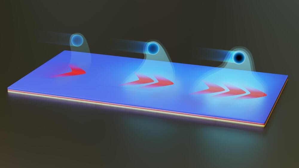
Officials from IBM and Samsung announced at this year’s IEDM conference in San Francisco a collaboration on a new chip design that adds transistors vertically on a chip. As part of their announcement, they suggested that their vertical transport field effect transistors (VTFET) could double the speed of processor chips, or alternatively, reduce the power they use by up to 85 percent.

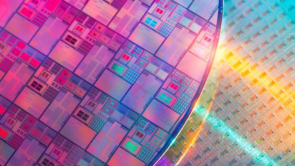
Since the beginning of digital technology, processing chips have been made by placing tiny transistors on a chip and connecting them. Over time, engineers have placed increasingly more transistors on chips that have remained roughly the same size—adhering, generally, to Moore’s Law, which states that the number of transistors on a should double every year. Engineers have known for a long time that there are limits to Moore’s Law—eventually, it would become impossible to add even one more transistor, much less double the number that are there.

So researchers are looking for other ways to make chips. But in the meantime, engineers continue to look for ways to add more transistors to conventional chips. In their announcement, IBM and Samsung have explained that they are taking steps to begin designing chips that can expand vertically. In a practical sense, the move was inevitable. As an analogy, when towns grew too big to be efficient, engineers began making buildings taller, essentially turning 2D towns into 3D cities. Officials and engineers at IBM and Samsung (and doubtless other corporations, such as Intel) suggest that now is the time to begin doing the same with microprocessors.

This 8-bit processor built in Minecraft can run its own games

The months-long project demonstrates the physics behind the CPUs we take for granted.


Computer chips have become so tiny and complex that it’s sometimes hard to remember that there are real physical principles behind them. They aren’t just a bunch of ever-increasing numbers. For a practical (well, virtual) example, check out the latest version of a computer processor built exclusively inside the Minecraft game engine.

Minecraft builder “Sammyuri” spent seven months building what they call the Chungus 2, an enormously complex computer processor that exists virtually inside the Minecraft game engine. This project isn’t the first time a computer processor has been virtually rebuilt inside Minecraft, but the Chungus 2 (Computation Humongous Unconventional Number and Graphics Unit) might very well be the largest and most complex, simulating an 8-bit processor with a one hertz clock speed and 256 bytes of RAM.

Minecraft processors use the physics engine of the game to recreate the structure of real processors on a macro scale, with materials including redstone dust, torches, repeaters, pistons, levers, and other simple machines. For a little perspective, each “block” inside the game is one virtual meter on each side, so recreating this build in the real world would make it approximately the size of a skyscraper or cruise ship.

IBM and Samsung say their new chip design could lead to week-long battery life on phones

Stacking transistors could be the next big thing in chips.


IBM and Samsung have announced their latest advance in semiconductor design: a new way to stack transistors vertically on a chip (instead of lying flat on the surface of the semiconductor).

The new Vertical Transport Field Effect Transistors (VTFET) design is meant to succeed the current FinFET technology that’s used for some of today’s most advanced chips and could allow for chips that are even more densely packed with transistors than today. In essence, the new design would stack transistors vertically, allowing for current to flow up and down the stack of transistors instead of the side-to-side horizontal layout that’s currently used on most chips.

Vertical designs for semiconductors have been a trend for a while (FinFET already offers some of those benefits); Intel’s future roadmap also looks to move in that direction, too, although its initial work focused on stacking chip components rather than individual transistors. It makes sense, after all: when you’ve run out of ways to add more chips in one plane, the only real direction (other than physically shrinking transistor technology) is to go up.

Coordinated Gene Expression and Chromatin Regulation during Hydra Head Regeneration

Abstract. The cnidarian model organism Hydra has long been studied for its remarkable ability to regenerate its head, which is controlled by a head organizer located near the hypostome. The canonical Wnt pathway plays a central role in head organizer function during regeneration and during bud formation, which is the asexual mode of reproduction in Hydra. However, it is unclear how shared the developmental programs of head organizer genesis are in budding and regeneration. Time-series analysis of gene expression changes during head regeneration and budding revealed a set of 298 differentially expressed genes during the 48-h head regeneration and 72-h budding time courses. In order to understand the regulatory elements controlling Hydra head regeneration, we first identified 27,137 open-chromatin elements that are open in one or more sections of the organism body or regenerating tissue. We used histone modification ChIP-seq to identify 9,998 candidate proximal promoter and 3,018 candidate enhancer-like regions respectively. We show that a subset of these regulatory elements is dynamically remodeled during head regeneration and identify a set of transcription factor motifs that are enriched in the enhancer regions activated during head regeneration. Our results show that Hydra displays complex gene regulatory structures of developmentally dynamic enhancers, which suggests that the evolution of complex developmental enhancers predates the split of cnidarians and bilaterians.

Evidence for Parallel Universes — Max Tegmark / Serious Science

Physicist Max Tegmark on predictions that cannot be observed, explanation of Universe’ fine tuning, and quantum computer.

You can now become our Patron and help us communicate science to a wider audience. Support us on https://www.patreon.com/SeriousScience.

Be the first to find out about our new videos and articles. Learn interesting facts about various topics and people. Discover the answers to the big questions. Be in the know.
Follow us:
Serious Science — http://serious-science.org/videos/1435
Patreon — https://www.patreon.com/SeriousScience.
Facebook — https://www.facebook.com/serious.scie
Twitter — https://twitter.com/scienceserious.
Instagram — https://www.instagram.com/serious.sci
Tumblr — http://serious-science.tumblr.com/
Vk — https://vk.com/seriousscience

Amazon Web Services faces second outage in weeks

A widespread outage at Amazon Web Services disrupted various websites and streaming platforms Wednesday — the second AWS outage reported in recent weeks.

More than 22,000 people had reported issues with the tech giant’s cloud computing service by 10:45 a.m. Monday, according to Downdetector.

The company acknowledged it was investigating connectivity issues in Northern California and Oregon. Between 11:10 and 11:14 a.m., it said the issues had been resolved.

Flawed Diamonds May Provide Perfect Interface for Quantum Computers — Faster and More Secure

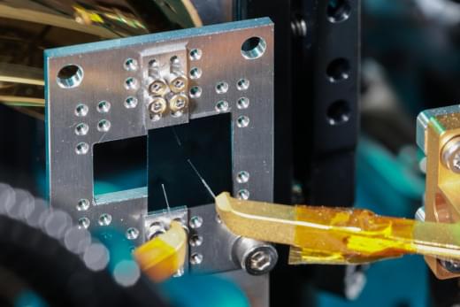
Flaws in diamonds — atomic defects where carbon is replaced by nitrogen or another element — may offer a close-to-perfect interface for quantum computing 0, a proposed communications exchange that promises to be faster and more secure than current methods. There’s one major problem, though: these flaws, known as diamond nitrogen-vacancy centers, are controlled via magnetic field, which is incompatible with existing quantum devices. Imagine trying to connect an Altair, an early personal computer developed in 1974, to the internet via WiFi. It’s a difficult, but not impossible task. The two technologies speak different languages, so the first step is to help translate.

Researchers at Yokohama National University have developed an interface approach to control the diamond nitrogen-vacancy centers in a way that allows direct translation to quantum devices. They published their method today (December 15, 2021) in Communications Physics.

“To realize the quantum internet, a quantum interface is required to generate remote quantum entanglement by photons, which are a quantum communication medium,” said corresponding author Hideo Kosaka, professor in the Quantum Information Research Center, Institute of Advanced Sciences and in the Department of Physics, Graduate School of Engineering, both at Yokohama National University. “.

Dell’s Concept Luna shows how future laptops could be easier to repair and recycle

Working with Intel, Dell has created a new laptop called Concept Luna with the aim of making future PCs easier to repair, reuse and recycle. Dell said that if it incorporated all the design ideas, it could reduce a computer’s carbon footprint by up to 50 percent compared to current laptop models.

A key feature of Concept Luna is the redesigned components and a new, more efficient layout. To start with, the motherboard is 75 percent smaller at just 5,580 square millimeters and has a 20 percent lower component count. Everything is rearranged, with the motherboard close to the top cover to expose it to a larger cooling area. It’s also separated from the battery charging unit in the base, allowing better passive cooling that could eliminate the need for a fan.

The extra efficiencies also reduce power requirements, allowing the designers to use a smaller battery with deep-cycle cells that offer a “long charge that can be maintained across many years of use, increasing refurbishment and reuse beyond the first product life it services,” Dell said.