A group of 51 superconducting qubits have been entangled inside a quantum computer, not just in pairs but in a complex system that entangles each qubit to every other one.
A group of 51 superconducting qubits have been entangled inside a quantum computer, not just in pairs but in a complex system that entangles each qubit to every other one.
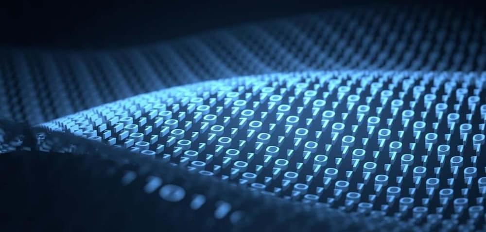
It’s estimated that humans are producing the equivalent of 10 million Blu-ray Discs of data per day – and all and zero of those have to be stored somewhere.
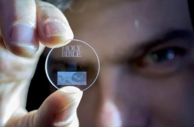
Now, UK researchers may have a solution: a five-dimensional (5D) digital data disc that can store 360 terabytes of data for about 13.8 billion years.
To create the data discs, scientists at the University of Southampton used a process called femtosecond laser writing, which creates tiny discs of glass using ultrafast lasers that generate short and intense pulses of light.
Brain tissue is one of the most intricate tissue specimens that scientists have arguably ever dealt with. Packed with an immeasurable amount of information, the human brain is the most sophisticated computational device with its network of around 86 billion neurons.
Understanding such complexity is a difficult task, and therefore making progress requires technologies to unravel the tiny, complex interactions taking place in the brain at microscopic scales. Imaging is therefore an enabling tool in neuroscience.
The new imaging and virtual reconstruction technology developed by Johann Danzl’s group, at the Institute of Science and Technology Austria (ISTA), is a big leap in imaging brain activity and is aptly named LIONESS—Live Information Optimized Nanoscopy Enabling Saturated Segmentation. Their work has been published in Nature Methods.
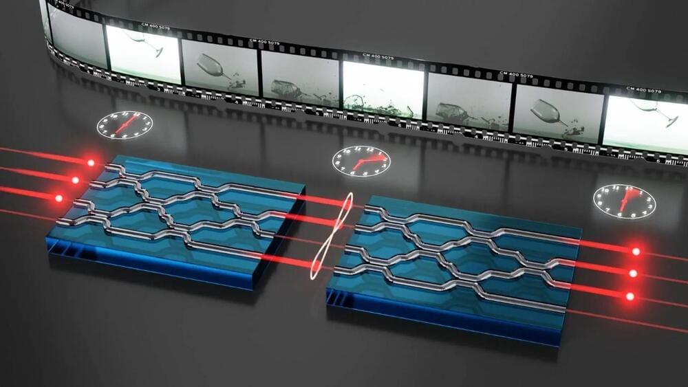
It seems quantum mechanics and thermodynamics cannot be true simultaneously. In a new publication, University of Twente researchers use photons in an optical chip to demonstrate how both theories can be true at the same time.
In quantum mechanics, time can be reversed and information is always preserved. That is, one can always find back the previous state of particles. It was long unknown how this could be true at the same time as thermodynamics. There, time has a direction and information can also be lost. “Just think of two photographs that you put in the sun for too long, after a while you can no longer distinguish them,” explains author Jelmer Renema.
There was already a theoretical solution to this quantum puzzle and even an experiment with atoms, but now the University of Twente (UT) researchers have also demonstrated it with photons. “Photons have the advantage that it is quite easy to reverse time with them,” explains Renema. In the experiment, the researchers used an optical chip with channels through which the photons could pass. At first, they could determine exactly how many photons there were in each channel, but after that, the photons shuffled positions.

“I find it totally amazing that it is possible at all to build these light structures.”
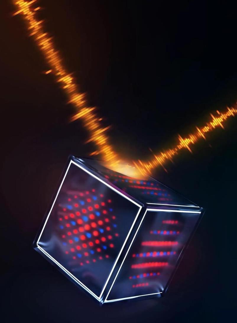
A Ph.D. candidate at has developed an innovative technique for creating the elementary building blocks of a future quantum computer or internet in a more controlled manner, opening up a potential solution to many of the challenges along the road to this long-sought technology.
Petr Steindl’s doctoral thesis, which he defended last week as the final step in his Ph.D. program at Leiden University in Germany, explores a new technique for generating photons using quantum dots and microcavities.

A better world without Facebook and all its negative impacts would be a significant step forward. Facebook’s dominance and influence have often been associated with issues such as privacy breaches, the spread of misinformation, and the erosion of real social connections. By breaking free from Facebook’s grip, we can foster a healthier online environment that prioritizes privacy, genuine interactions, and reliable information. It is time to envision a world where social media platforms serve as catalysts for positive change, promoting authentic communication and meaningful connections among individuals.
(Image credit: Adobe Stock)
Mark Zuckerberg, the co-founder of Facebook (now Meta), recently celebrated reaching 100 million users in just five days with his new Twitter-like platform called Threads. However, this achievement doesn’t impress me much. Instead, it highlights Zuckerberg’s tendency to imitate rather than innovate.
While I used to admire him, I now realize that he doesn’t belong in the same league as my true idols. Comparing the 100 million sign-ups for ChatGPT to the 100 million Threads users is simply absurd.
Researchers have achieved a major milestone in quantum computing by extending the lifetime of quantum information beyond the breakeven point using Quantum Error Correction, opening the path for effective quantum information processing amidst real-world noise. Understanding Decoherence and Quantum E.
Summary: Our brains have been likened to an orchestra, with neurons as musicians creating a symphony of thought and memory.
A recent study reveals the conductor behind this symphony: electric fields. These fields are generated by the combined electrical activity of neurons, orchestrating them into functional networks.
This research shines a light on the brain’s complex inner workings and could impact the future of brain-computer interfaces.
Researchers in the Andrew and Erna Viterbi Faculty of Electrical and Computer Engineering have demonstrated control over an emerging material, which they consider as a possible future alternative to silicon in microelectronics. This is a timely development, because scientists and engineers face challenges in continuing the transistor shrinking trend, an important driver of computer chip performance.
The continuous performance improvement of these chips has been driven by shrinking the size of the most basic logic “Lego” piece – the transistor. Transistors are miniature switches that control the flow of electric currents, analogous to a faucet controlling the flow of water. Already in the early 1960s, Gordon Moore, the founder of Intel, proposed that the transistors’ miniaturization rate should allow doubling of the number of transistors per area every 2 years.
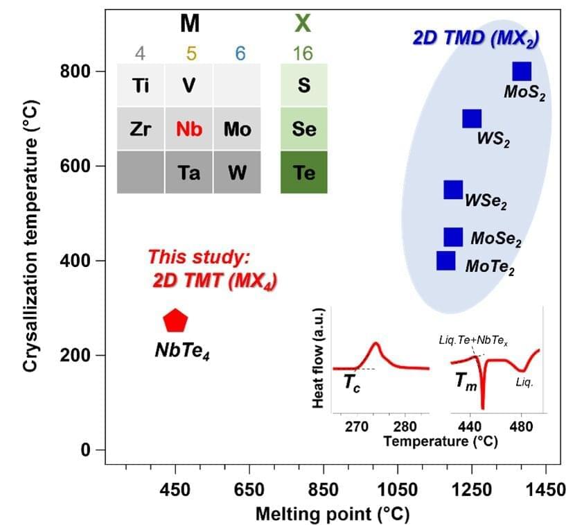
Phase change memory is a type of nonvolatile memory that harnesses a phase change material’s (PCM) ability to shift from an amorphous state, i.e., where atoms are disorganized, to a crystalline state, i.e., where atoms are tightly packed close together. This change produces a reversible electrical property which can be engineered to store and retrieve data.
While this field is in its infancy, phase change memory could potentially revolutionize data storage because of its high storage density, and faster read and write capabilities. But still, the complex switching mechanism and intricate fabrication methods associated with these materials have posed challenges for mass production.
In recent years, two-dimensional (2D) Van Der Waals (vdW) transition metal di-chalcogenides have emerged as a promising PCM for usage in phase change memory.