Toggle light / dark theme

I wonder if you could use this stuff for brain scans.


Neuralink, the US neurotechnology firm co-founded by billionaire entrepreneur Elon Musk, has begun recruiting key employees to run its clinical trials, signaling that it’s inching closer to starting human testing of its brain implants.

The company has posted advertisements to hire a clinical trial director and a clinical trial coordinator. The ads note that the staffers will “work closely with some of the most innovative doctors and top engineers, as well as working with Neuralink’s first clinical trial participants.” Neuralink said the director will lead and help build its clinical research team and will develop “regulatory interactions that come with a fast-paced and ever-evolving environment.”

Musk, who ranks as the world’s richest person with a fortune estimated at $256 billion, said last month that he expects to have Neuralink brain chips implanted in humans sometime in 2022, pending approval for testing plans by the US Food and Drug Administration (FDA).

‘Geometric frustration’ can cause the electrons in materials with atoms arranged in a triangular pattern to organize in three competing ways simultaneously, reveals a new computational study led by researchers at the Flatiron Institute.

Materials that look like mosaics of triangular tiles at the atomic level sometimes have paradoxical properties, and quantum physicists have finally found out why.

Using a combination of cutting-edge computational techniques, the scientists found that under special conditions, these triangular-patterned materials can end up in a mashup of three different phases at the same time. The competing phases overlap, with each wrestling for dominance. As a result, the material counterintuitively becomes more ordered when heated up, the scientists reported in Physical Review X.

High-resolution recordings of electrical signals from the surface of the brain could improve surgeons’ ability to remove brain tumors and treat epilepsy, and could open up new possibilities for medium-and longer-term brain-computer interfaces.

A team of engineers, surgeons, and medical researchers has published data from both humans and rats demonstrating that a new array of brain sensors can record electrical signals directly from the surface of the human brain in record-breaking detail. The new brain sensors feature densely packed grids of either 1,024 or 2,048 embedded electrocorticography (ECoG) sensors. The paper was published by the journal Science Translational Medicine on January 19, 2022.

In today’s video I show you how the Neurosity Crown works by making a prototype to control lights which is initiated by thinking about movement of my left arm.

This Brain Computer Interface video will cover these areas:
👉 Neurosity console overview.
👉 Neurosity console left arm thoughts training with Kinesis.
👉 Extending Unity Notion SDK to subscribe to Kinesis updates and therefore get the data into Unity for further usage.
👉 Simple LightController in Unity to turn on and off lights controlled by a Philips Hue Hub.

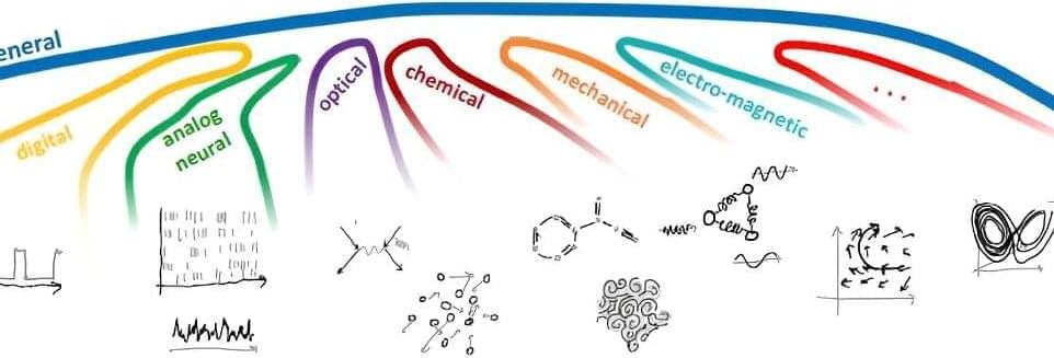
Computers play an important role in many aspects of life today. Digital computers are the most widely used, while quantum computers are well known. However, the least known computers are the so-called Stochastic Pulse Computers. Their work is based on highly parallel logical operations between trains of electrical pulses, where the pulses occur at random times, as in neurons, the nerve cells in the brains of humans and mammals.

Elon Musk’s Neuralink, the company that purports to implant computer chips in human brains, just took a critical step toward actually following through.

The brain implant firm is officially hiring a clinical trial director, which means Musk’s futuristic firm is finally ready, at least on its own terms, to give next-gen brain-computer interfaces (BCIs) a try.

Intel has selected Ohio for a new chip manufacturing complex that would cost at least $20 billion, ramping up an effort to increase U.S. production of computer chips as users grapple with a lingering shortage of the vital components.

Intel said Friday that the new site near Columbus would initially have two chip factories and would directly employ 3,000 people, while creating additional jobs in construction and at nearby businesses.

Patrick Gelsinger, who became Intel’s chief executive last year, has rapidly increased the company’s investments in manufacturing to help reduce U.S. reliance on foreign chip makers while lobbying Congress to pass incentives aimed at increasing domestic chip production. He has said that Intel might invest as much as $100 billion over a decade in its next U.S. manufacturing campus, linking the scope and speed of that expansion to expected federal grants if Congress approves a spending package known as the CHIPS Act.

BERKELEY, Calif. 0, Jan. 20, 2022 — Atom Computing, the creators of the first quantum computer made of nuclear-spin qubits from optically-trapped neutral atoms, today announced closure of a $60M Series B round. Third Point Ventures led the round, followed by Primer Movers Lab and insiders including Innovation Endeavors, Venrock and Prelude Ventures. Following the completion of their first 100-qubit quantum computing system with world-record 40 second coherence times, Atom Computing will use this new investment to build their second-generation quantum computing systems and commercialize the technology.

“Atom Computing designed and built our first-generation machine, Phoenix 0, in less than two years and our team was the fastest to deliver a 100-qubit system,” said Rob Hays 0, CEO and President, Atom Computing. “We gained valuable learnings from the system and have proven the technology. The investment announced today accelerates the commercialization opportunities and we look forward to bringing this to market.”

With this new level of investment, the company will turn its focus to developing much larger systems that are required to run commercial use-cases with paradigm-shifting compute performance.

ASML President and CTO Martin van den Brink said:

“Intel’s vision and early commitment to ASML’s High-NA EUV technology is proof of its relentless pursuit of Moore’s Law. Compared to the current EUV systems, our innovative extended EUV roadmap delivers continued lithographic improvements at reduced complexity, cost, cycle time and energy that the chip industry needs to drive affordable scaling well into the next decade.”

Intel plans to start high-volume manufacturing (HVM) in 2025, which is also when the company will be using its 18A (1.8nm) fabrication technology. To do so, Intel has been experimenting for quite a while when it first obtained ASML’s Twinscan EXE:5000, which was the industry’s first EUV scanner with a 0.55 numerical aperture. Today, the company ordered ASML’s next-generation High-NA tool, the Twinscan EXE:5200.