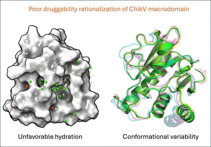
The chikungunya virus (ChikV) was first isolated during an arthritic disease outbreak in Tanzania in 1952 [1, 2]. ChikV is a mosquito-borne virus that belongs to the Alphavirus genus of the Togaviridae family. ChikV infections have emerged as a global health risk with approximately 16.9 million cases per year [3]. Major symptoms of ChikV infection include severe fever, rashes, and joint pain. Chronic arthritis-like symptoms may persist and can be debilitating [4, 5]. ChikV, a positive-sense RNA virus, encodes 5 structural proteins and 4 nonstructural proteins (NSP1 to NSP4) [6]. Nonstructural protein 3 (NSP3) consists of a conserved macrodomain (Mac1) at the N-terminus, a poorly conserved hypervariable domain, and a central zinc-binding domain known as the alphavirus unique domain [7]. The macrodomain fold is highly conserved across evolution, having been identified in bacteria, algae, and eukaryotes [8, 9]. It has been suggested that ChikV Mac1 suppresses the host immune response through its adenosine diphosphate ribosyl (ADP-ribosyl) hydrolase activity [10], which removes ADP-ribose posttranslational modifications from target host proteins by hydrolyzing mono-ADP-ribosylated aspartate and glutamate residues. Mac1 has therefore emerged as a promising antiviral drug target [10], supported by evidence suggesting that it is a key determinant of ChikV virulence in mice. Despite their therapeutic potential, efforts to identify ChikV inhibitors have had limited success. A fragment screen of ~14,000 compounds identified only weak inhibitors (e.g., 2-pyrimidone-4-carboxylic acid scaffold, with one of the compounds showing IC50 of 23 μM) [11]. Another computational docking and simulation study screened 820 compounds and predicted that natural compounds from plants, including apigetrin, baicalin, baloxavir, luteoloside, rutaecarpine, and amentoflavone [12], are Mac1 inhibitors. The predicted binding affinity of baicalin was −10.8 kcal/mol against ChikV Mac1. Another study identified N-[2-(5-methoxy-1 H-indol-3-yl) ethyl]-2-oxo-1,2-dihydroquinoline-4-carboxamide through virtual screening of 245,532 natural compounds, followed by in vitro validation using a microscale thermophoresis binding assay (binding constant [Kd] of 1.066 × 10⁻⁶ ± 0.95 μM) and in vivo inhibition of ChikV replication [13].
Similar to ChikV, severe acute respiratory syndrome coronavirus 2 (SARS-CoV-2) NSP3 contains 3 tandem macrodomains, with Mac1 serving as the catalytically active macrodomain that binds and hydrolyzes mono-ADP-ribose on posttranslationally modified target host proteins [14,15]. SARS-CoV-2 Mac1 is essential for viral pathogenesis and represents a promising drug target [16,17]. In contrast to ChikV Mac1, it has proven amenable to inhibitor development. An early crystallographic screen of approximately 2,600 compounds revealed 234 fragment structures bound to SARS-CoV-2 Mac1 [18]. Using these hits, several optimized inhibitors were designed, followed by another round of crystallographic screening [19]. Among the resulting top inhibitors was AVI-4206, a potent inhibitor with an IC50 of 20 nM that is effective in an animal model of SARS-CoV-2 infection [20]. Other studies have identified additional promising scaffolds, including 2-amide-3-methylester thiophene scaffold derivatives that bind SARS-CoV-2 Mac1 (IC50 = 1.5 μM) and inhibit viral replication [21], synthetic analogs of ADP-ribose that bind SARS-CoV-2 Mac1 with nanomolar affinity [22], and pyrrolo-pyrimidine-based compounds that inhibit viral replication in SARS-CoV-2 [23].
The structural similarity between ChikV Mac1 and SARS-CoV-2 Mac1 [24] has not translated into similar druggability. One strategy to improve ligand-binding affinity is to exploit the presence of water molecules in the binding site by designing inhibitors that effectively use them to form bridging interactions that strengthen binding to the protein [25]. This strategy is particularly relevant for Mac1 ADP-ribose-binding sites, which are large, solvent exposed, and known to maintain an extensive network of ordered water molecules upon ADP binding. In SARS-CoV-2 Mac1, ADP-ribose forms several water-mediated interactions, resulting in the water network in the ADP-ribose-binding site reorganizing upon ligand binding [18,26].