Following successful early demonstrations of linking two quantum computing chips, IBM is aiming to break records for the largest quantum computer yet by combining many of them in parallel.
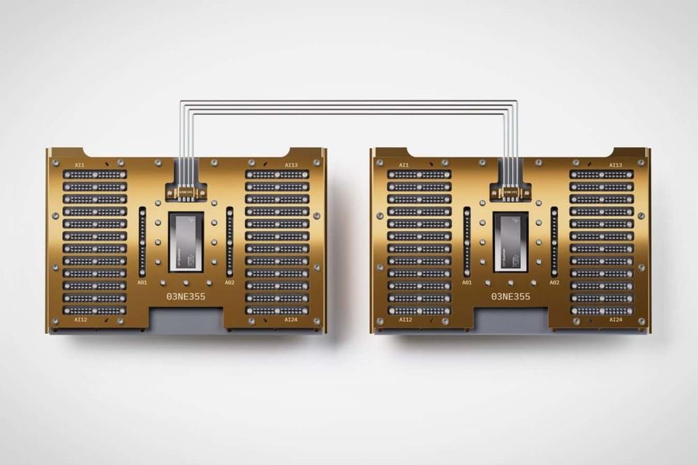
Following successful early demonstrations of linking two quantum computing chips, IBM is aiming to break records for the largest quantum computer yet by combining many of them in parallel.


A quantum state of light has been successfully teleported through more than 30 kilometers (around 18 miles) of fiber optic cable amid a torrent of internet traffic – a feat of engineering once considered impossible.
The impressive demonstration by researchers in the US may not help you beam to work to beat the morning traffic, or download your favourite cat videos faster.
However, the ability to teleport quantum states through existing infrastructure represents a monumental step towards achieving a quantum-connected computing network, enhanced encryption, or powerful new methods of sensing.

Physicists uncovered a fascinating link between the Large Hadron Collider and quantum computing. They found that top quarks produced at the LHC exhibit a property called “magic,” essential for quantum computation.
This discovery could revolutionize our understanding of quantum mechanics and its applications, bridging the gap between quantum theory and particle physics.
Quantum Computing and the Power of “Magic”

Texas Instruments has announced a tranche of federal CHIPS Act funding worth up to $1.6 billion, a show of support for a semiconductor manufacturing industry that’s becoming more entrenched in North Texas.
Texas Instruments also expects to receive somewhere between $6 billion and $8 billion in U.S. Treasury tax credits for manufacturing investments, and up to $10 million to boost workforce development.
All told, the money will assist in funding three new Texas Instruments plants: two based in Sherman and one in Lehi, Utah, creating 2,000 new jobs. Separately, Samsung will receive as much as $4.75 billion in CHIPS Act money, a figure Bloomberg notes was below what was originally envisaged.

In a pioneering move for quantum technology, Nanyang Technological University (NTU) and the National University of Singapore (NUS) have launched AQSolotl, a deep-tech startup presenting CHRONOS-Q —a state-of-the-art quantum controller designed to integrate classical computing systems with quantum computers. This innovation positions Singapore at the forefront of the global quantum ecosystem, with wide-ranging applications across industries.
CHRONOS-Q tackles the complexity of controlling quantum computers by acting as a translator between classical and quantum systems. It enables efficient control via standard computing devices, features an intuitive interface, and significantly reduces operational barriers, paving the way for broader adoption. Its modular, compact design ensures scalability and suitability for diverse environments, from research labs to mobile quantum setups.
With groundbreaking speed—determining qubit states in under 14 nanoseconds—and customizable firmware, CHRONOS-Q promises cost-effective, future-proof solutions for academia and industry. The startup’s founders, including Professor Rainer Dumke from NTU and CEO Patrick Bore, emphasize the transformative potential of accessible quantum computing for solving global challenges.

Users of Google’s Chrome browser can rest easy knowing that their surfing is secure, thanks in part to cryptographer Joppe Bos. He’s coauthor of a quantum-secure encryption algorithm that was adopted as a standard by the U.S. National Institute of Standards and Technology (NIST) in August and is already being implemented in a wide range of technology products, including Chrome.
Rapid advances in quantum computing have stoked fears that future devices may be able to break the encryption used by most modern technology. These approaches to encryption typically rely on mathematical puzzles that are too complex for classical computers to crack. But quantum computers can exploit quantum phenomena like superposition and entanglement to compute these problems much faster, and a powerful enough machine should be able to break current encryption.
Understand the key concepts of Quantum Physics and the Multiverse in 15 minutes.