Page 9564
Aug 18, 2018
What Causes Glaucoma? Scientists May Have Finally Figured It Out
Posted by Genevieve Klien in category: biotech/medical
Researchers say an autoimmune response may be behind the eye pressure and vision loss that sometimes precedes a glaucoma diagnosis.
Aug 18, 2018
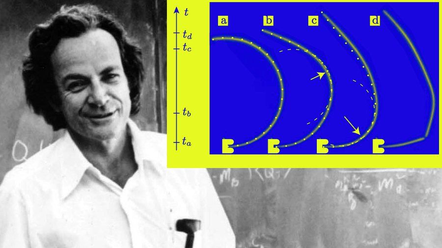
The snapback effect: Richard Feynman’s famed physics puzzle finally gets solved
Posted by Genevieve Klien in category: physics
Aug 18, 2018
These beautiful works of art illustrate the brain’s complexity
Posted by Genevieve Klien in category: neuroscience

Art is sometimes the easiest way of understanding the mysterious and unknowable.
The Art of Neuroscience competition, organized by the Netherlands Institute for Neuroscience, solicited entries from around the world to help “make the research from neuroscience labs more tangible…[and] for scientists to evaluate their own work from a different perspective.” The recognized entries come from practicing scientists presenting their work in creative ways as well as artists who have collaborated with scientists.
Continue reading “These beautiful works of art illustrate the brain’s complexity” »
Aug 18, 2018
High-efficiency large-area perovskite photovoltaic modules achieved via electrochemically assembled metal-filamentary nanoelectrodes
Posted by Genevieve Klien in categories: solar power, sustainability
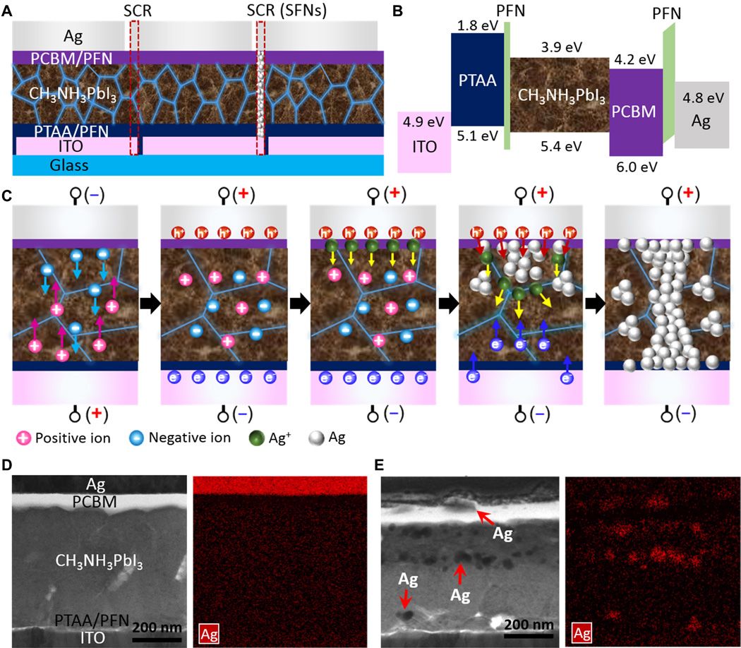
Realizing industrial-scale, large-area photovoltaic modules without any considerable performance losses compared with the performance of laboratory-scale, small-area perovskite solar cells (PSCs) has been a challenge for practical applications of PSCs. Highly sophisticated patterning processes for achieving series connections, typically fabricated using printing or laser-scribing techniques, cause unexpected efficiency drops and require complicated manufacturing processes. We successfully fabricated high-efficiency, large-area PSC modules using a new electrochemical patterning process. The intrinsic ion-conducting features of perovskites enabled us to create metal-filamentary nanoelectrodes to facilitate the monolithic serial interconnections of PSC modules. By fabricating planar-type PSC modules through low-temperature annealing and all-solution processing, we demonstrated a notably high module efficiency of 14.0% for a total area of 9.06 cm with a high geometric fill factor of 94.1%.
The unprecedented features of organic-inorganic hybrid perovskite semiconductors, which allow low-temperature crystal film growth from their precursor solutions, have greatly promoted both scientific and technological revolutions in a wide range of fields within electronics (1, 2). The advent of organolead trihalide perovskite semiconductors as light harvesters has resulted in the fastest-advancing solar technology to date, with an extremely rapid rise in power conversion efficiency (PCE) from 3.8 to 22.1% over just a few years (3–6). In addition to recent remarkable breakthroughs in addressing the instability of these devices, which has been considered the greatest challenge toward commercialization due to their intrinsic properties vulnerable to oxygen and moisture, pioneering researchers have begun fabricating large-area devices for their ultimate application (7–16).
Aug 18, 2018
Next Windows 10 update nearing completion as it gets its official name
Posted by Genevieve Klien in category: futurism
Aug 18, 2018
Scientists Are Developing a Unique Identifier for Your Brain
Posted by Genevieve Klien in categories: genetics, life extension, neuroscience
A neurological “functional fingerprint” allows scientists to explore the influence of genetics, environment and aging on brain connectivity.
Aug 18, 2018
Photo Tour: Inside Boeing’s CST-100 Starliner Spaceship Hangar
Posted by Sean Brazell in category: space travel
I pilot. I fly. wink
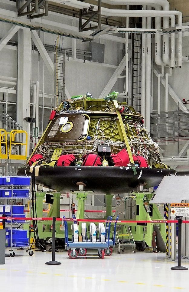
Take a look inside the CST-100 Starliner hangar, where Boeing is building the private space capsules that will fly NASA astronauts and more into space! This photo shows an exterior view of the Boeing Starliner Facility, which once housed the space shuttle Discovery.
Aug 18, 2018
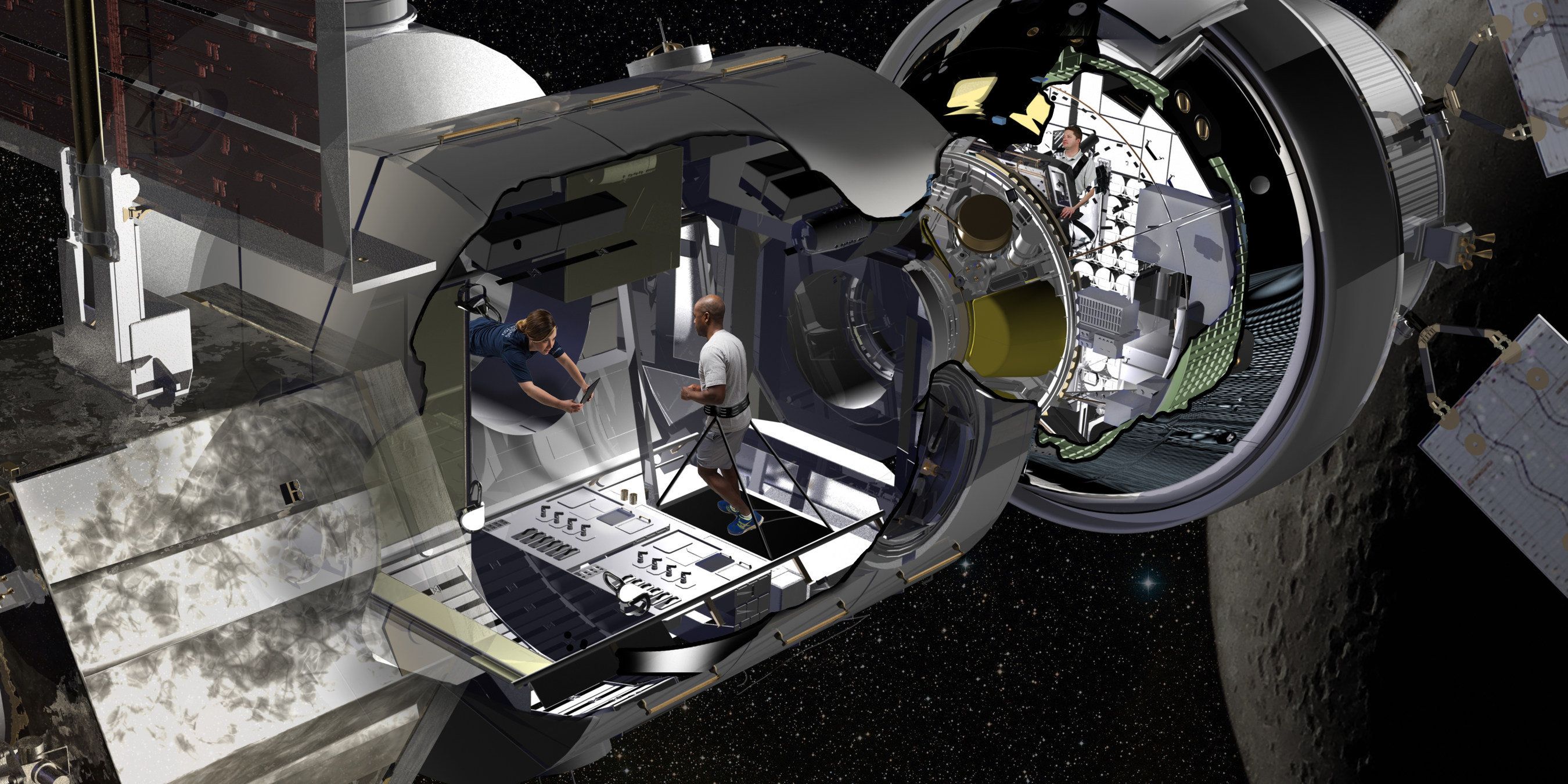
Lockheed Martin gives first look into where astronauts may live on missions to deep space
Posted by Genevieve Klien in categories: habitats, space
A massive cylindrical habitat may one day house up to four astronauts as they make the trek to deep space.
Lockheed Martin gave a first look at what one of these habitats might look like Thursday at the Kennedy Space Center, where the aerospace giant is under contract with NASA to build a prototype of the living quarters.
Lockheed is one of six contractors—the others are Boeing, Sierra Nevada Corp.‘s Space Systems, Orbital ATK, NanoRacks and Bigelow Aerospace—that NASA awarded a combined $65 million to build a habitat prototype by the end of the year. The agency will then review the proposals to reach a better understanding of the systems and interfaces that need to be in place to facilitate living in deep space.
Aug 18, 2018
Nvidia’s new Turing architecture is all about real-time ray tracing and AI
Posted by Genevieve Klien in categories: innovation, robotics/AI

In recent days, word about Nvidia’s new Turing architecture started leaking out of the Santa Clara-based company’s headquarters. So it didn’t come as a major surprise that the company today announced during its Siggraph keynote the launch of this new architecture and three new pro-oriented workstation graphics cards in its Quadro family.
Nvidia describes the new Turing architecture as “the greatest leap since the invention of the CUDA GPU in 2006.” That’s a high bar to clear, but there may be a kernel of truth here. These new Quadro RTx chips are the first to feature the company’s new RT Cores. “RT” here stands for ray tracing, a rendering method that basically traces the path of light as it interacts with the objects in a scene. This technique has been around for a very long time (remember POV-Ray on the Amiga?). Traditionally, though, it was always very computationally intensive, though the results tend to look far more realistic. In recent years, ray tracing got a new boost thanks to faster GPUs and support from the likes of Microsoft, which recently added ray tracing support to DirectX.
Continue reading “Nvidia’s new Turing architecture is all about real-time ray tracing and AI” »
