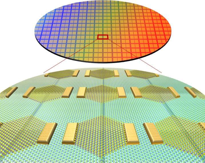
A research team led by Director JO Moon-Ho of the Center for Van der Waals Quantum Solids within the Institute for Basic Science (IBS) has implemented a novel method to achieve epitaxial growth of 1D metallic materials with a width of less than 1 nanometer (nm). The group applied this process to develop a new structure for 2D semiconductor logic circuits. Notably, they used the 1D metals as a gate electrode of the ultra-miniaturized transistor.
This research was published in the journal Nature Nanotechnology (“Integrated 1D epitaxial mirror twin boundaries for ultra-scaled 2D MoS 2 field-effect transistors”).
Integrated devices based on two-dimensional (2D) semiconductors, which exhibit excellent properties even at the ultimate limit of material thickness down to the atomic scale, are a major focus of basic and applied research worldwide. However, realizing such ultra-miniaturized transistor devices that can control the electron movement within a few nanometers, let alone developing the manufacturing process for these integrated circuits, has been met with significant technical challenges.


Leave a reply