Jun 28, 2023
New mass spectrometry combo offers promise for tapping nature’s unknown chemical universe
Posted by Shailesh Prasad in categories: biotech/medical, chemistry
The universe is awash in billions of possible chemicals. But even with a bevy of high-tech instruments, scientists have determined the chemical structures of just a small fraction of those compounds, maybe 1%.
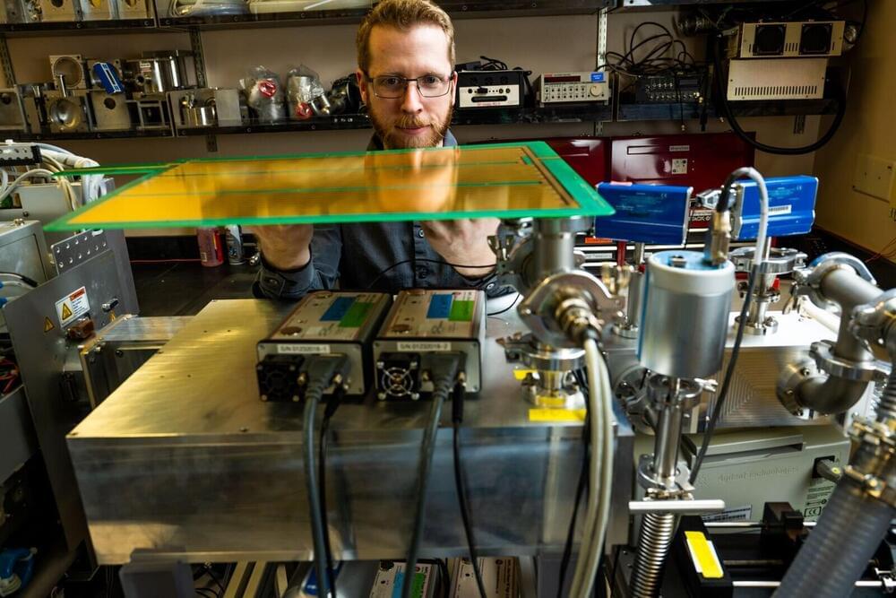
Scientists at the Department of Energy’s Pacific Northwest National Laboratory (PNNL) are taking aim at the other 99%, creating new ways to learn more about a vast sea of unknown compounds. There may be cures for disease, new approaches for tackling climate change, or new chemical or biological threats lurking in the chemical universe.
The work is part of an initiative known as m/q, or “m over q” —shorthand for mass divided by charge, which signifies one of the ways that scientists measure chemical properties in the world of mass spectrometry.


