Page 11963
Sep 16, 2015
8 Printable Martian Habitat Designs That We Want To Live In
Posted by Shailesh Prasad in categories: habitats, space
Sep 16, 2015
Future’s 10 Mind-Blowing Scenarios for Interstellar Travel
Posted by Shailesh Prasad in categories: business, media & arts, space travel

Time for Humanity to discover what’s outside the backyard… (HD — 12/2014)
FOLLOW THE HYBRID LIBRARIAN:
Subscribe ▶ http://bit.ly/daretoknow
Facebook ▶ http://on.fb.me/170IAJK
Twitter ▶ http://bit.ly/14vhMgZ
Google+ ▶ http://bit.ly/15eoHil
Tumblr ▶ http://bit.ly/11UtNr1
Continue reading “Future’s 10 Mind-Blowing Scenarios for Interstellar Travel” »
Sep 16, 2015
Nanodiamonds Formed In A Carbon Cage
Posted by Shailesh Prasad in category: nanotechnology
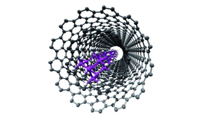
Scientists have successfully synthesized diamond-like nanomaterials in the hollow of a carbon nanotube.
Asian Scientist Newsroom | September 16, 2015 | In the Lab.
Sep 16, 2015
MIT creates diode for light, makes photonic silicon chips possible
Posted by Shailesh Prasad in categories: computing, electronics, mobile phones, transportation
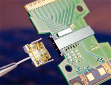
Light-emitting diodes (LEDs) are a cornerstone of consumer tech. They make thin-and-light TVs and smartphones possible, provide efficient household, handheld, and automobile illumination, and, of course, without LEDs your router would not have blinkenlights. Thanks to some engineers from MIT, though, a new diode looks set to steal the humble LED’s thunder. Dubbed a diode for light, and crafted using standard silicon chip fabrication techniques, this is a key discovery that will pave the path to photonic (as opposed to electronic) pathways on computer chips and circuit boards.
In electronics, a diode is a gate that only allows electrons to pass in one direction (and with an LED, it also emits light at the same time). In this case, the diode for light — which is made from a thin layer of garnet — is transparent in one direction, but opaque in the other. Garnet is usually hard to deposit on a silicon wafer, but the MIT researchers found a way to do it — and that’s really the meat of this discovery.
![]() Basically, it’s now possible, with regular chip-fab tools, to create an integrated silicon circuit with optical, rather than electronic, interconnects — both internally, and between other chips. Photons, moving through the kind of transparent metamaterials that would be required to make such a circuit, move a lot faster than electrons. Furthermore, optical channels, through wavelength-division multiplexing, can carry a lot more data than electric signals. At the moment, hundreds of copper wires connect the CPU, northbridge, and memory — with on-chip photonic controllers, a motherboard might only have 10 or 20 channels.
Basically, it’s now possible, with regular chip-fab tools, to create an integrated silicon circuit with optical, rather than electronic, interconnects — both internally, and between other chips. Photons, moving through the kind of transparent metamaterials that would be required to make such a circuit, move a lot faster than electrons. Furthermore, optical channels, through wavelength-division multiplexing, can carry a lot more data than electric signals. At the moment, hundreds of copper wires connect the CPU, northbridge, and memory — with on-chip photonic controllers, a motherboard might only have 10 or 20 channels.
Sep 16, 2015
New Solar Panels That Work At Night
Posted by Shailesh Prasad in categories: materials, nanotechnology, solar power, sustainability
Despite the enormous untapped potential of solar energy, one thing is for sure- photovoltaics are only as good as the sun’s rays shining upon them. However, researchers at the Idaho National Laboratory are close to the production of a super-thin solar film that would be cost-effective, imprinted on flexible materials, and would be able to harvest solar energy even after sunset!


Sep 16, 2015
Silicon Valley billionaires are appalled
Posted by Shailesh Prasad in category: education
Sep 16, 2015
Will You Join the Transhuman Evolution?
Posted by Lily Graca in categories: business, evolution, transhumanism
DLD (Digital-Life-Design) is a global network on innovation, digitization, science and culture which connects business, creative and social leaders, opinion-formers and influencers for crossover conversation and inspiration.
Replacing metal wiring with fiber optics could change everything from supercomputers to laptops.


