Aug 31, 2016
DARPA Researchers Develop Novel Method for Room-Temperature Atomic Layer Deposition
Posted by Karen Hurst in category: materials
Nice.
DARPA-supported researchers have developed a new approach for synthesizing ultrathin materials at room temperature—a breakthrough over industrial approaches that have demanded temperatures of 800 degrees Celsius or more. The advance opens a path to creating a host of previously unattainable thin-film microelectronics, whose production by conventional methods has been impossible because many components lose their critical functions when subjected to high temperatures.
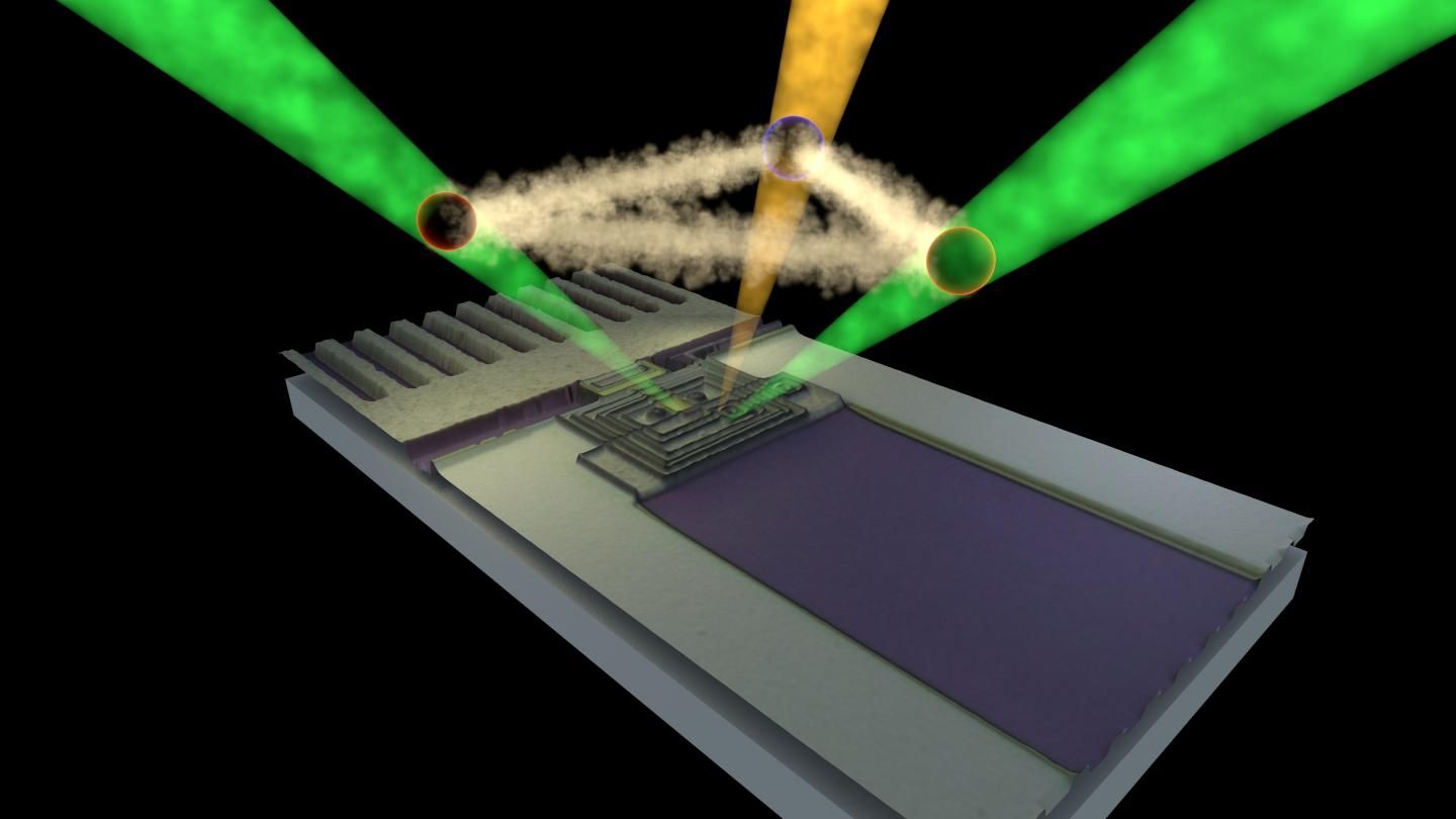
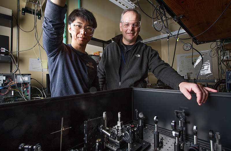
The new method, known as electron-enhanced atomic layer deposition (EE-ALD), was recently developed at the University of Colorado, Boulder (CU) as part of DARPA’s Local Control of Materials Synthesis (LoCo) program. The CU team demonstrated room-temperature deposition of silicon and gallium nitride—linchpin elements in many advanced microelectronics—as well as the ability to controllably etch specific materials, leading to precise spatial control in three dimensions. Such a capability is critical as the demand grows for ever-smaller device architectures.
After first demonstrating the process in early 2015, team members went on to perform detailed mechanistic studies to learn how best to exploit and control EE-ALD for film growth. By controlling the electron energy during the ALD cycles, they discovered that they could tune the process to favor either material deposition or removal. The ability to selectively remove (etch) deposited material with electrons under conditions as low as room temperature is unprecedented and is anticipated to enhance film quality. The group is also exploring other methods to etch specific materials—such as aluminum nitride and hafnium oxide, important in specialized electronics applications—showing that they can selectively etch these materials in composites, which provides an attractive alternative to traditional masking approaches.
