Apr 21, 2024
Meta’s New GenAI Is Theatrical. Here’s How To Make It Valuable
Posted by Gemechu Taye in categories: materials, robotics/AI
Concern about a generative AI bubble is growing. To defend against disillusionment, measure its concrete value.
Concern about a generative AI bubble is growing. To defend against disillusionment, measure its concrete value.
FineWeb: 15 trillion tokens of high quality web data the web has to offer.
The 🍷 dataset consists of more than 15T tokens of cleaned and deduplicated english web data from CommonCrawl.
We’re on a journey to advance and democratize artificial intelligence through open source and open science.
The LASSIE project is preparing for a time when people and robots explore space together.
Learn more about how the #space economy can improve life on #Earth from our new insight report, ‘Space: The $1.8 Trillion Opportunity for Global Economic Growth’:
Space is approaching a new frontier. The space economy is expected to be worth $1.8 trillion by 2035 as satellite and rocket-enabled technologies become increasingly prevalent, according to a new report.
Continue reading “Space is booming. Here’s how to embrace the $1.8 trillion opportunity” »
Everyone is in a big hurry to get the latest and greatest GPU accelerators to build generative AI platforms. Those who can’t get GPUs, or have custom devices that are better suited to their workloads than GPUs, deploy other kinds of accelerators.
The companies designing these AI compute engines have two things in common. First, they are all using Taiwan Semiconductor Manufacturing Co as their chip etching foundry, and many are using TSMC as their socket packager. And second, they have not lost their minds. With the devices launched so far this year, AI compute engine designers are hanging back a bit rather than try to be on the bleeding edge of process and packaging technology so they can make a little money on products and processes that were very expensive to develop.
Nothing shows this better than the fact that the future “Blackwell” B100 and B200 GPU accelerators from Nvidia, which are not even going to start shipping until later this year, are based on the N4P process at Taiwan Semiconductor Manufacturing Co. This is a refined variant of the N4 process that the prior generation of “Hopper” H100 and H200 GPUs used, also a 4 nanometer product.
Construction is the world’s largest industry, employing seven percent of the planet’s working-age adults, contributing 13 percent of the world’s GDP and completing floor space equivalent to the city of Paris every seven days.
The construction industry is also the most inefficient, least digitised and most polluting industry (37% of ALL emissions), so change is imperative from macro economic necessity alone. For the builders of the world faced with a jigsaw puzzle of partial digital solutions and chronic labor and supply chain issues, the margins are growing ever-thinner and the necessity is to change or perish.
British company Automated Architecture (AUAR) has a thoroughly ingenious solution and it has enlisted an all-star cast of financial backers in short order: Morgan Stanley, ABB Robotics, Rival Holdings (USA), Vandenbussche NV (Belgium) with VCs such as Miles Ahead and Bacchus Venture Capital (Jim Horowitz et al) helping to get the initial idea off the ground.
The “it” Mr Woodman is referring to is Sora, a new text-to-video AI model from OpenAI, the artificial intelligence research organisation behind viral chatbot ChatGPT.
Instead of using their broad technical skills in filmmaking, such as animation, to overcome obstacles in the process, Mr Woodman and his team relied only on the model to generate footage for them, shot by shot.
“We just continued generating and it was almost like post-production and production in the same breath,” says Patrick Cederberg, who also worked on the project.
Meta CEO Mark Zuckerberg thinks ‘feedback loops,’ the process of AI learning from its own outputs, are more important than new data for developing AI.
Marshal Brain’s 2003 book Manna was quite ahead of its time in foreseeing that eventually, one way or another, we will have to confront and address the phenomenon of technological unemployment. In addition, Marshall is a passionate brainiac with a jovial personality, impressive background and a unique perspective. And so I was very happy to meet him in person for an exclusive interview. [Special thanks to David Wood without whose introduction this interview may not have happened!]
During our 82 min conversation with Marshall Brain we cover a variety of interesting topics such as: his books The Second Intelligent Species and Manna; AI as the end game for humanity; using cockroaches as a metaphor; logic and ethics; simulating the human brain; the importance of language and visual processing for the creating of AI; marrying off Siri to Watson; technological unemployment, social welfare and perpetual vacation; capitalism, socialism and the need for systemic change …
As always you can listen to or download the audio file above or scroll down and watch the video interview in full. To show your support you can write a review on iTunes, make a direct donation or become a patron on Patreon.
A dog-like, bio-inspired robot called Spirit is still learning to walk, but could one day be deployed on the moon to explore steep, potentially hazardous areas with a team of robot companions.

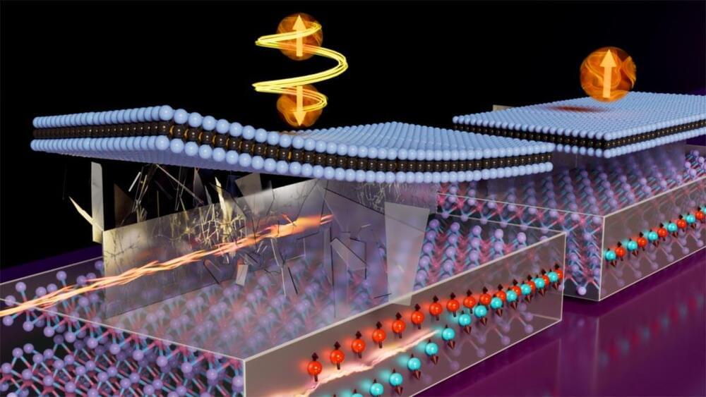
MIT scientists have tackled key obstacles to bringing 2D magnetic materials into practical use, setting the stage for the next generation of energy-efficient computers.
Globally, computation is booming at an unprecedented rate, fueled by the boons of artificial intelligence. With this, the staggering energy demand of the world’s computing infrastructure has become a major concern, and the development of computing devices that are far more energy-efficient is a leading challenge for the scientific community.
Continue reading “MIT Unlocks the Power of 2D Magnets for Future Computing” »
