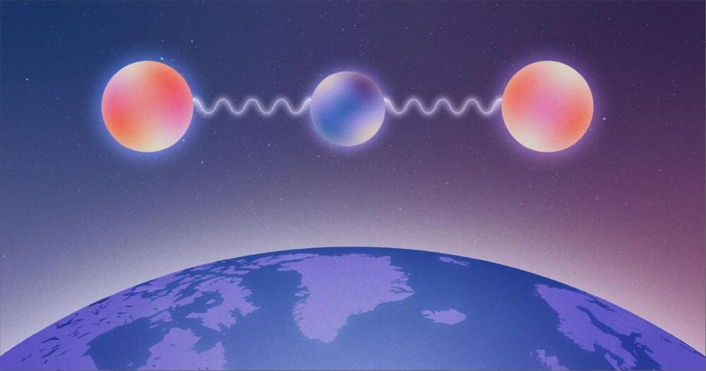
An answer to a decades-old question in the theory of quantum entanglement raises more questions about this quirky phenomenon.
Physicists have a long list of open problems they consider important for advancing the field of quantum information. Problem 5 asks whether a system can exist in its maximally entangled state in a realistic scenario, in which noise is present. Now Julio de Vicente at Carlos III University of Madrid has answered this fundamental quantum question with a definitive “no” [1]. De Vicente says that he hopes his work will “open a new research avenue within entanglement theory.”
From quantum sensors to quantum computers, many technologies require quantum mechanically entangled particles to operate. The properties of such particles are correlated in a way that would not be possible in classical physics. Ideally, for technology applications, these particles should be in the so-called maximally entangled state, one in which all possible measures of entanglement are maximized. Scientists predict that particles can exist in this state in the absence of experimental, environmental, and statistical noise. But it was unclear whether the particles could also exist in a maximally entangled state in real-world scenarios, where noise is unavoidable.


