Oct 29, 2022
Novel thermal phases of topological quantum matter in the lab
Posted by Dan Breeden in categories: computing, particle physics, quantum physics
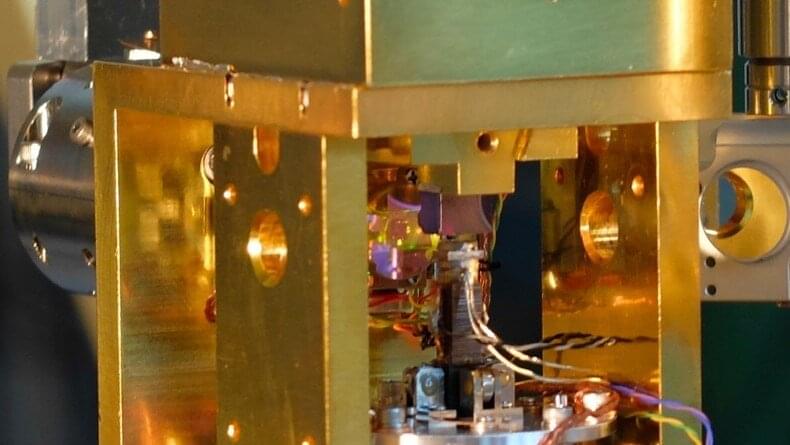
For the first time, a group of researchers from Universidad Complutense de Madrid, IBM, ETH Zurich, MIT and Harvard University have observed topological phases of matter of quantum states under the action of temperature or certain types of experimental imperfections. The experiment was conducted using quantum simulator at IBM.
Quantum simulators were first conjectured by the Nobel Prize laureate Richard Feynman in 1982. Ordinary classical computers are inefficient at simulating systems of interacting quantum particles These new simulators are genuinely quantum and can be controlled very precisely. They replicate other quantum systems that are harder to manipulate and whose physical properties remain very much unknown.
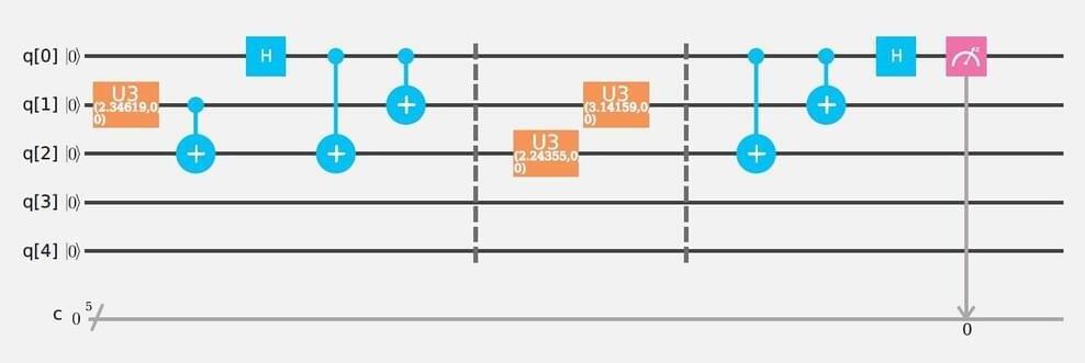
In an article published in the journal Quantum Information, the researchers describe using a quantum simulator with superconducting qubits at IBM to replicate materials known as topological insulators at finite temperature, and measure for the first time their topological quantum phases.
